• Chinese Journal of Lasers
  • Vol. 47, Issue 12, 1202007 (2020)
Chen Ni, Yan Bo, Li Zhenjun, Li Liang, and He Ning*
Author Affiliations
  • College of Mechanical and Electrical Engineering, Nanjing University of Aeronauticsand Astronautics, Nanjing, Jiangsu 210016, China
  • show less
    DOI: 10.3788/CJL202047.1202007 Cite this Article Set citation alerts
    Chen Ni, Yan Bo, Li Zhenjun, Li Liang, He Ning. Gaussian Pulsed Laser Etching of CVD Diamonds[J]. Chinese Journal of Lasers, 2020, 47(12): 1202007 Copy Citation Text show less
    Schematic of device for nanosecond laser processing of CVD diamonds
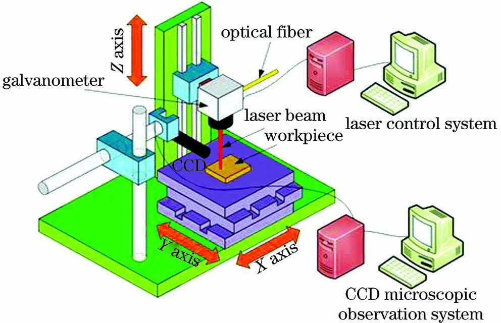
    Fig. 1. Schematic of device for nanosecond laser processing of CVD diamonds
    Simulation temperature cloud after single pulse. (a) Horizontal direction; (b) vertical direction
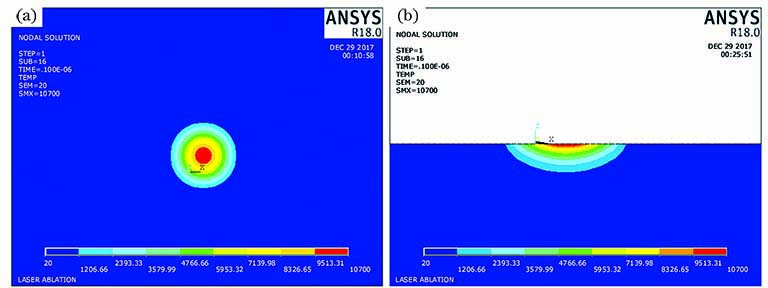
    Fig. 2. Simulation temperature cloud after single pulse. (a) Horizontal direction; (b) vertical direction
    Effect of laser power on etching surface pit morphology. (a) 3W; (b) 4W; (c) 5W; (d) 7W
    Fig. 3. Effect of laser power on etching surface pit morphology. (a) 3W; (b) 4W; (c) 5W; (d) 7W
    Raman spectra
    Fig. 4. Raman spectra
    Morphology of etching pit. (a) Optical morphology; (b) Gaussian fitting of profile
    Fig. 5. Morphology of etching pit. (a) Optical morphology; (b) Gaussian fitting of profile
    Effect of scanning speed on pulse spot overlapping during laser line etching. (a) Relatively small scanning speed; (b) relatively large scanning speed
    Fig. 6. Effect of scanning speed on pulse spot overlapping during laser line etching. (a) Relatively small scanning speed; (b) relatively large scanning speed
    Laser line etching energy density model
    Fig. 7. Laser line etching energy density model
    Line etching widths and side etching depths under different laser scanning speeds. (a) 50mm·s-1; (b) 20mm·s-1; (c) 0.2mm·s-1
    Fig. 8. Line etching widths and side etching depths under different laser scanning speeds. (a) 50mm·s-1; (b) 20mm·s-1; (c) 0.2mm·s-1
    Effect of laser power on line etching width. (a) 3W; (b) 7W; (c) 15W
    Fig. 9. Effect of laser power on line etching width. (a) 3W; (b) 7W; (c) 15W
    Effect of laser power on side surface line etching depth. (a) 3W; (b) 7W; (c) 15W
    Fig. 10. Effect of laser power on side surface line etching depth. (a) 3W; (b) 7W; (c) 15W
    SEM image of laser etched CVD diamond surface. (a) Surface; (b) side surface
    Fig. 11. SEM image of laser etched CVD diamond surface. (a) Surface; (b) side surface
    ParameterPulse duration/nsRepetition rate/kHzBeam qualityfactorWavelength/nmAveragepower /WFocus radius/μm
    Value10020--2001.510642--2020
    Table 1. Main parameters of pulsed Ytterbium-doped fiber laser
    No.Number of pulsesPower /W
    1253, 4, 5, 7
    220, 50, 100, 2003
    Table 2. Experimental parameters of laser point etching
    No.Scanning speed /(mm·s-1)Power /W
    30.2, 20.0, 50.04
    4203, 7, 15
    Table 3. Experimental parameters of laser line etching
    Power /WDepth /μmWidth /μmR-square
    3-5.1910.380.97
    4-9.9718.340.99
    5-16.1132.080.98
    7-19.2938.040.97
    Table 4. Gaussian fitting results of etching profiles under different laser powers
    Number of pulsesDepth /μmWidth /μmR-square
    25-5.1910.380.97
    50-8.1115.140.99
    100-10.3422.460.97
    200-15.4031.020.99
    Table 5. Gaussian fitting results of etching profiles under different numbers of pulses
    Chen Ni, Yan Bo, Li Zhenjun, Li Liang, He Ning. Gaussian Pulsed Laser Etching of CVD Diamonds[J]. Chinese Journal of Lasers, 2020, 47(12): 1202007
    Download Citation