
Yu Li, Weifang Yuan, Ke Li, Xiaofeng Duan, Kai Liu, Yongqing Huang. InGaAs/InAlAs SAGCMCT avalanche photodiode with high linearity and wide dynamic range[J]. Chinese Optics Letters, 2022, 20(2): 022503
- Chinese Optics Letters
- Vol. 20, Issue 2, 022503 (2022)
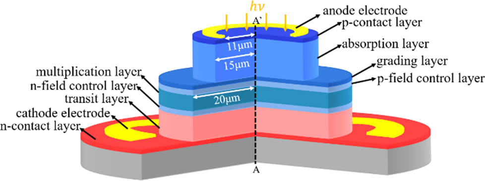
Fig. 1. Layer structure of the InGaAs/InAlAs SAGCMCT-APD.
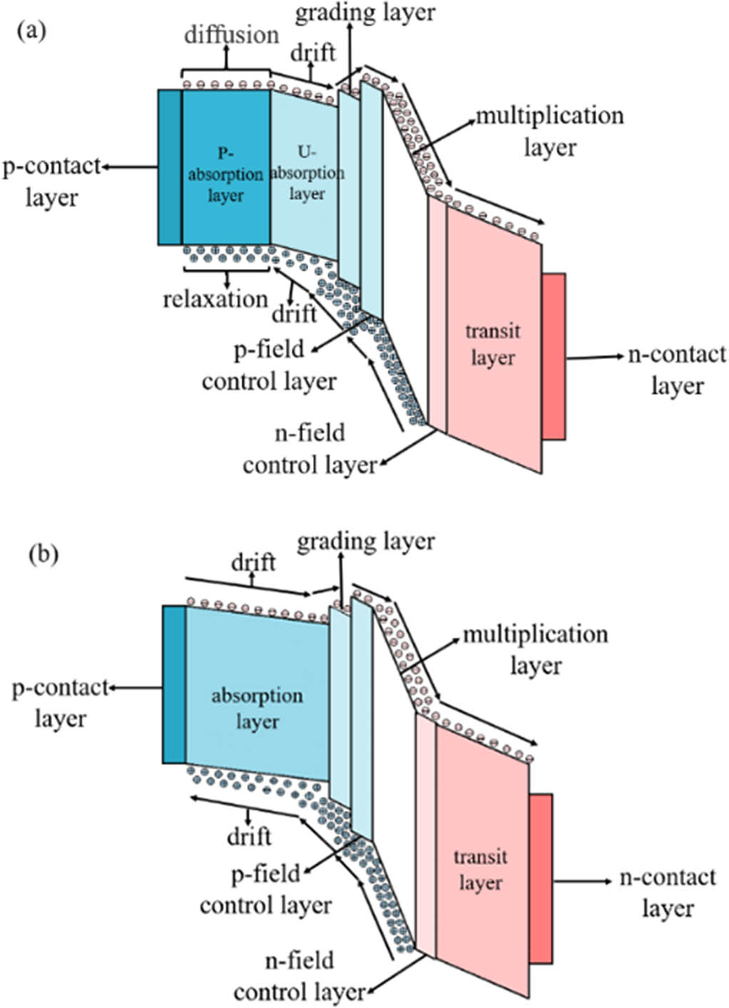
Fig. 2. (a) Band diagram of the hybrid absorption layer APD under high input optical power and (b) band diagram of the APD with only one absorption layer under high input optical power.
Fig. 3. Simulated vertical direction (A-A’) (a) electric field distribution and (b) electrons and holes concentration distributions at the input optical power of 0.001 mW and 4.5 mW.
Fig. 4. (a) Simulated vertical direction (A-A’) electric field distribution of the device, (b) energy band schematic diagram of the absorption layer, (c) absorption layer band diagram at 0.9Vbr under different R values, and (d) simulated hole and electron concentration distribution in the vertical direction (A-A’) at R = 0.2 and R = 0.8 under the input optical power of 0.5 mW.
Fig. 5. Simulated input optical power dependence of linearity compression at the gain of 10 under different R values.
Fig. 6. Simulated vertical direction (A-A’) (a) electric field distribution and (b) absorption layer band diagram of the device under different absorption layer doping levels; (c) simulated hole and electron concentration distribution in the vertical direction (A-A’) of the device at the gain of 10 under different absorption layer doping levels.
Fig. 7. Simulated optical input power dependence of linearity compression at the gain of 10 under different absorption layer doping levels.
Fig. 8. (a) Simulated photocurrent and gain of the device under different absorption layer doping levels and (b) simulated bandwidth of the device at the gain of 10 under different absorption layer doping levels. Compared with Ref. [15], the 1 dB compression point is −3.38 dBm, and the bandwidth is 6.7 GHz. Our optimized device obtains a bandwidth of 8 GHz.
|
Table 1. Material Parameters in the Simulation
|
Table 2. Structure Parameters of the SAGCMCT-APD

Set citation alerts for the article
Please enter your email address
© Copyright 2018-2021 | Chinese Laser Press. All Rights Reserved 沪ICP备15018463号-20