
Yu Li, Weifang Yuan, Ke Li, Xiaofeng Duan, Kai Liu, Yongqing Huang. InGaAs/InAlAs SAGCMCT avalanche photodiode with high linearity and wide dynamic range[J]. Chinese Optics Letters, 2022, 20(2): 022503
- Chinese Optics Letters
- Vol. 20, Issue 2, 022503 (2022)
Abstract
1. Introduction
Avalanche photodiodes (APDs) are widely used in optical communication systems. Compared with conventional photodiodes (PDs), APDs have a unique internal gain, which can achieve higher detection sensitivity[
To improve the linearity of APDs, it is necessary to solve the problem of hole accumulation under high input optical power. One of the effective ways to suppress the space charge effect is to use bandgap engineering. By changing the structure of the epitaxial layer and the doping level of each layer, the holes transport can be effectively accelerated, and the space charge effect can be alleviated. At present, there are two methods to alleviate the space charge effect by using bandgap engineering. Firstly, the bandgap difference between the M-layer and the absorption layer can be smoothed by adding a grading layer, which has been carefully studied by researchers[
In this paper, the linearity of APDs is improved by using bandgap engineering. The influence of the absorption layer on APD linearity is carefully studied, and two separated absorption, grading, charge, multiplication, charge, and transit (SAGCMCT)-APD models with different absorption layer structures are established. The InAlAs M-layer thickness is 200 nm. In the hybrid absorber device structure, increasing the proportion of the -type absorption layer can increase the 1 dB compression point from to . In the device structure with only one absorption layer, the 1 dB compression point can be enhanced from to 1.43 dBm by increasing the doping level of the absorption layer. Since increasing the doping level of the absorption layer will worsen the capacitance of the whole device, we adopted the SAGCMCT structure[
Sign up for Chinese Optics Letters TOC. Get the latest issue of Chinese Optics Letters delivered right to you!Sign up now
2. Device Structure
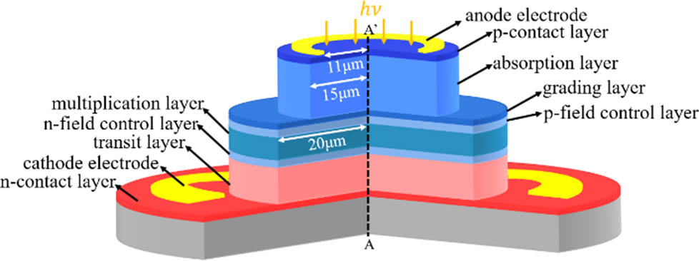
The epitaxial layer structure of the top-illuminated InGaAs/InAlAs SAGCMCT-APD is shown in Fig. 1. It consists of a p-type contact layer, InGaAs absorption layer, InAlGaAs grading layer, p-type field control layer, 200 nm InAlAs M-layer, n-type field control layer, and transit layer. The total thickness of the whole absorber is 500 nm. The diameter of the active region is 30 µm. The vertical central axis of the device is shown in A-A’. The mesa structure with a carefully designed diameter is used to limit the edge electric field of the M-layer. The p-type field control layer and n-type field control layer are used to adjust the electric field distribution of the whole device so that the M-layer maintains a high electric field. Since the transit velocity of holes is slower than that of electrons, adding a transit layer behind the n-type field control layer does not affect the transit bandwidth of the device, but it can increase the thickness of the depletion region and reduce the capacitance of the device.
![]()
Figure 1.Layer structure of the InGaAs/InAlAs SAGCMCT-APD.
A large number of electrons generated by the absorption layer will move to the M-layer and trigger an avalanche multiplication, causing the M-layer to produce more electron-hole pairs under high input optical power. The electrons generated in the M-layer will drift to the electrode and be collected, while a large number of holes can also be collected by moving through the transit layer and absorption layer. Due to the slow movement velocity of holes, they tend to accumulate and lead to a space charge effect. Therefore, in order to alleviate the space charge effect, the transportation of holes needs to be accelerated. The effect of the absorbing layer on alleviating the space charge effect is worthy of careful study.
To study the influence of the absorption layer on the linearity of APDs, we designed two kinds of absorption layer structures. One is a hybrid absorption layer structure, and the other has only one absorption layer. The total thickness of the absorption layer is 500 nm. Figures 2(a) and 2(b), respectively, show the band diagrams of the APD with these two structures under high input optical power. In the hybrid absorption layer structure, holes drift in the intrinsic absorption layer and relax directly in the -type absorption layer. The effect of the -type absorption layer thickness on the linearity of APDs can be explored. In the device structure with only one absorption layer, with the increase of the absorption layer doping level, the holes change from drift motion to direct relaxation, and the electrons change from drift motion to diffusion motion. The influence of the absorption layer doping level on the linearity of APDs can be explored.
![]()
Figure 2.(a) Band diagram of the hybrid absorption layer APD under high input optical power and (b) band diagram of the APD with only one absorption layer under high input optical power.
Results presented in this paper were obtained by the use of Silvaco technology computer aided design (TCAD). The Shockley–Read–Hall recombination model, Fermi–Dirac carrier statistics model, Auger recombination model, analytic concentration dependent mobility model, optical recombination model, Selberherr’s impact ionization model, and band-to-band tunneling model are used in this simulation[
| Parameters | Unit | InGaAs | InAlGaAs | InAlAs |
|---|---|---|---|---|
| Band-gap | eV | 0.75 | 0.99 | 1.44 |
| Electron affinity | eV | 4.5 | 4.38 | 4.25 |
| Permittivity | 13.9 | 12.5 | 12.2 | |
| SRH lifetime | s | |||
| Selberherr’s parameters An, Ap | cm−1 | |||
| Selberherr’s parameters Bn, Bp | V/cm | |||
| Selberherr’s parameter | 1 | 1 | 1 | 1 |
| Band-to-band parameter A | V−1·cm−1·s−1 | |||
| Band-to-band parameter B | V/cm | |||
| Band-to-band parameter | 1 | 2 | 2 | 2 |
Table 1. Material Parameters in the Simulation
Due to the space charge effect, the control effect of the field control layer on the electric field of APDs will be weakened under high input optical power. Thus, the electric field of the M-layer will be reduced, and the multiplication gain will also be decreased. Figures 3(a) and 3(b) show the simulated electric field distribution and the electron and hole concentration distribution in the vertical direction of the APD when the input optical power is 0.001 mW and 4.5 mW, respectively. When the input optical power is 4.5 mW, the electric field of the M-layer decreases by about 70 kV/cm, and the electric field of the absorption layer increases. This is because the accumulation of holes leads to the weakening of the control effect of the p-type field control layer on the electric field. This is consistent with the above analysis.
![]()
Figure 3.Simulated vertical direction (A-A’) (a) electric field distribution and (b) electrons and holes concentration distributions at the input optical power of 0.001 mW and 4.5 mW.
3. Simulation Results and Discussion
In this section, we established an SAGCMCT-APD model with a hybrid absorption layer structure, and the total absorption layer thickness is 500 nm. is used to represent the ratio of the p-type absorption layer thickness to the total absorption layer thickness. Figure 4(a) shows the simulated vertical direction (A-A’) electric field distribution of the device under different values. The electric field of the M-layer is very uniform, and the electric field intensity is about 640 kV/cm. The electric field range of the undoped absorption layer is between 88 kV/cm and 73 kV/cm, while the electric field intensity of the -type absorption layer is about 0 kV/cm. Due to the different thickness of the undoped absorption layer, the breakdown voltage () of the device is slightly different, but the gain of the device under operation is the same at about 10. Figure 4(b) shows the energy band schematic diagram of the absorption layer. is used to represent the thickness of the non-depletion absorption layer, and is used to represent the thickness of the depletion absorption layer.
![]()
Figure 4.(a) Simulated vertical direction (A-A’) electric field distribution of the device, (b) energy band schematic diagram of the absorption layer, (c) absorption layer band diagram at 0.9Vbr under different R values, and (d) simulated hole and electron concentration distribution in the vertical direction (A-A’) at R = 0.2 and R = 0.8 under the input optical power of 0.5 mW.
Figure 4(c) shows the absorption layer band diagram of the APD with a hybrid absorption layer structure at under different values. In the non-depleted absorption layer, the holes will relax directly, and, in the depleted absorption layer, the holes will drift. With the increase of non-depleted absorption layer thickness, the energy band will gradually be flattened, and the movement distance of holes will be shortened, which is beneficial to the transmission of holes. Figure 4(d) shows the simulated concentration distribution of the hole and electron in the vertical direction (A-A’) at and under the input optical power of 0.5 mW. At same input optical power, the hole concentration in the device at is larger than that at . This indicates that compared with , holes begin to accumulate when .
Figure 5 shows the simulated input optical power dependence of linearity compression at the gain of 10 under different values. The 1 dB compression points of the device increase gradually with the increase of R. When the thickness of the p-type absorption layer is 100 nm and 400 nm, the 1 dB compression points of the device are and , respectively. Under high input optical power, holes will accumulate, resulting in the space charge effect. The linearity of the device will be reduced. The absorption layer is a long distance for holes to transit. Increasing the thickness of the p-type absorption layer is equivalent to reducing the transmission distance of holes. The linearity of the device will be greatly improved.
![]()
Figure 5.Simulated input optical power dependence of linearity compression at the gain of 10 under different R values.
In this section, we established an SAGCMCT-APD model with only one absorption layer, and the thickness of the absorption layer is 500 nm. We set the doping level of the absorption layer to increase from to . Figure 6(a) shows the simulated vertical direction (A-A’) electric field distribution of the device under different absorption layer doping levels. The electric field intensity of the M-layer is about 610 kV/cm. Figure 6(b) shows the absorption layer band diagram under different absorption layer doping levels. With the increase of the absorption layer doping level, the electric field of the absorption layer decreases gradually, and the energy band gradually becomes flat. The holes change from drift motion to relaxation, which greatly reduces the transit time of holes in the absorption layer. Figure 6(c) shows the simulated concentration distribution of the hole and electron in the vertical direction (A-A’) of the device at the input optical power of 1 mW under different absorption layer doping levels. When the absorption layer doping level is , the hole concentration is significantly higher than that when the absorption layer doping level is under the same input optical power. When the incident light power is 1 mW, the device with the absorption layer doping level of has serious hole accumulation, which will produce a space charge effect and greatly affect the linearity of the device.
![]()
Figure 6.Simulated vertical direction (A-A’) (a) electric field distribution and (b) absorption layer band diagram of the device under different absorption layer doping levels; (c) simulated hole and electron concentration distribution in the vertical direction (A-A’) of the device at the gain of 10 under different absorption layer doping levels.
Figure 7 shows the simulated optical input power dependence of linearity compression at the gain of 10 under different absorption layer doping levels. With the increase of the doping level of the absorption layer, the 1 dB compression point of the device increases from to 1.43 dBm. These results indicate that the rapid transport of holes in the absorption layer plays an important role in reducing the space charge effect and improving the linearity of the device at high input optical power.
![]()
Figure 7.Simulated optical input power dependence of linearity compression at the gain of 10 under different absorption layer doping levels.
From Fig. 8(a), when the input optical power is 1.5 mW, the photocurrent of the device increases with the increasing doping levels of the absorption layer. The gain of the device can also be improved. Figure 8(b) shows the simulation bandwidth of the device at the gain of 10 under different absorption layer doping levels. The 3 dB bandwidth of the device is about 8 GHz to 8.5 GHz. Compared with Ref. [15], the 1 dB compression point is , and the bandwidth is 6.7 GHz. Our optimized device obtains a bandwidth of 8 GHz and a 1 dB compression point of 1.43 dBm. The final optimized structure parameters of the SAGCMCT-APD are shown in Table 2.
| Layer | Thickness (nm) | Doping ( |
|---|---|---|
| P-InGaAs contact layer | 50 | |
| InGaAs absorption layer | 500 | |
| InAlGaAs grading layer | 50 | |
| P-InAlAs field control layer | 70 | |
| InAlAs M-layer | 200 | |
| N-InAlAs field control layer | 70 | |
| InP-transit layer | 350 | |
| N-InGaAs contact layer | 50 |
Table 2. Structure Parameters of the SAGCMCT-APD
![]()
Figure 8.(a) Simulated photocurrent and gain of the device under different absorption layer doping levels and (b) simulated bandwidth of the device at the gain of 10 under different absorption layer doping levels. Compared with Ref. [
4. Conclusions
In summary, the space charge effect can be alleviated, and the linearity of APDs can be improved by using bandgap engineering. The absorption layer is also crucial for improving the linearity of APDs because the holes need to be transmitted in a thicker absorption layer. In the hybrid absorption layer structure, increasing the ratio of the p-type absorption layer thickness to the total absorption layer thickness can shorten the transit time of holes and improve the linearity of APDs. In the single absorption layer structure, increasing the doping level of the absorption layer can also make the holes shift from drift motion to relaxation and improve the linearity of the device. In the APD designed with only one absorption layer, the 1 dB compression point can reach 1.43 dBm when the doping level is set to . The device achieves 8 GHz bandwidth at a gain of 10. The improvement principle is similar to UTC-PD with high linearity.
References
[1] L. E. Tarof, J. Yu, R. Bruce, D. G. Knight, T. Baird, B. Oosterbrink. High-frequency performance of separate absorption grating, charge, and multiplication InP/InGaAs avalanche photodiodes. IEEE Photon. Technol. Lett., 5, 672(1993).
[2] C. Liao, J. Wang, H. Lu, X. Peng, J. Guo, R. Li, Z. Wei, J. Zhou, J. Feng, S. Liu. Experimental characterization improving the design of InGaAs/InP APD for single photon detection. Chin. Opt. Lett., 3, S31(2005).
[3] P. Zhou, C. Liao, Z. Wei, C. Li, S. Yuan. Determination of breakdown voltage of In0.53Ga0.47As/InP single photon avalanche diodes. Chin. Opt. Lett., 9, 010402(2011).
[4] J. C. Campbell, S. Demiguel, F. Ma, A. Beck, X. Zheng, X. Li, J. D. Beck, M. A. Kinch, A. Huntington, L. A. Coldren, J. Decobert, N. Tscherptner. Recent advances in avalanche photodiodes. IEEE J. Sel. Top. Quantum Electron., 10, 777(2004).
[5] J. C. Campbell. Recent advances in avalanche photodiodes. J. Lightwave Technol., 34, 278(2016).
[6] M. Nada, Y. Yamada, H. Matsuzaki. A high-linearity avalanche photodiodes with a dual-carrier injection structure. IEEE Photonics Technol. Lett., 29, 1828(2017).
[7] M. Nada, T. Hoshi, H. Yamazaki, T. Hashimoto, H. Matsuzaki. Linearity improvement of high-speed avalanche photodiodes using thin depleted absorber operating with higher order modulation format. Opt. Express., 23, 27715(2015).
[8] M. Nada, T. Yoshimatsu, Y. Muramoto, H. Yokoyama, H. Matsuzaki. Design and performance of high-speed avalanche photodiodes for 100-Gb/s systems and beyond. J. Lightwave Technol., 33, 984(2015).
[9] L. Zhang, Y. Yang, W. Xia, X. Zhu, W. Chen, Y. Lu. Linearity of quadrant avalanche photodiode in laser tracking system. Chin. Opt. Lett., 7, 728(2009).
[10] T. Tsutsumi, T. Sakamoto, Y. Sakai, T. Fujiwara, H. Ou, Y. Kimura, K. Suzuki. Long-reach and high-splitting-ratio 10G-EPON system with semiconductor optical amplifier and N:1 OSU protection. J. Lightwave Technol., 33, 1660(2015).
[11] M. Nada, M. C. Chen, H. Katsurai, Y. Nakanishi, K. Sano. Practically implementable high-sensitivity 10-Gbit/s avalanche photodiode using inverted p-down design. IEICE Electron Expr., 18, 20210142(2021).
[12] A. Beling, H. Pan, H. Chen, J. C. Campbell. Measurement and modeling of a high-linearity modified unitraveling carrier photodiode. IEEE Photon. Technol. Lett., 20, 1219(2008).
[13] W. Sun, Y. Fu, Z. Lu, J. C. Campbell. Study of bandwidth enhancement and non-linear behavior in avalanche photodiodes under high power condition. J. Appl. Phys., 113, 044509(2013).
[14] C. Wu, J. Zhang, X. Peng, W. Qian. Improving the detection range of APD detection system by waveform integration. Infrared Laser Eng., 49, 20200149(2020).
[15] C. Shen, L. Yang, H. Guo, D. Yang, L. Chen, L. He. Numerical simulation of high-operating-temperature MWIR HgCdTe APD detectors. J. Infrared Millim. Waves, 40, 576(2021).
[16] D. Zheng, X. Su, Y. Xu, Z. Niu. High gain and low dark current AlInAsSb avalanche photodiodes grown by quaternary digital alloys. J. Infrared Millim. Waves, 40, 172(2021).
[17] M. Nada, T. Hoshi, H. Yamazaki, T. Hashimoto, H. Matsuzaki. Linearity improvement of high-speed avalanche photodiodes using thin depleted absorber operating with higher order modulation format. Opt. Express, 23, 27715(2015).
[18] Y. Jiang, J. Chen. Optimization of the Linearity of InGaAs/InAlAs SAGCM APDs. J. Lightwave Technol., 37, 3459(2019).
[19] H. Wang, X. Yang, R. Wang, T. He, K. Liu. Low dark current and high gain-bandwidth product of avalanche photodiodes: optimization and realization. Opt. Express, 28, 16211(2020).
[20] . ATLAS User’s Manual Device Simulation Software(2010).
[21] O. S. Abdulwahid, J. Sexton, I. Kostakis, K. Ian, M. Missous. Physical modelling and experimental characterisation of InAlAs/InGaAs avalanche photodiode for 10 Gb/s data rates and higher. IET Optoelectron., 12, 5(2018).

Set citation alerts for the article
Please enter your email address
© Copyright 2018-2021 | Chinese Laser Press. All Rights Reserved 沪ICP备15018463号-20