
Meicheng Fu, Yi Zheng, Gaoyuan Li, Wenjun Yi, Junli Qi, Shaojie Yin, Xiujian Li, Xiaowei Guan. Ultra-compact titanium dioxide micro-ring resonators with sub-10-μm radius for on-chip photonics[J]. Photonics Research, 2021, 9(7): 1416
- Photonics Research
- Vol. 9, Issue 7, 1416 (2021)
Abstract
1. INTRODUCTION
Microring resonators (MRRs) are indispensable and may be the most versatile elements in photonic integrated circuits (PICs) for applications ranging from conventional optical signal processing [1] and optical sensors [2] to emerging quantum information processing [3] and optical computing [4]. MRRs with an ultracompact footprint, e.g., radius will not only benefit the integration density of PICs, but also provide large nonlinear field enhancement () and large Purcell factors (), which are of great importance for the nonlinear devices [5] and light sources [6], respectively. Waveguides with high linear refractive index (RI) are essential for ultracompact MRRs; otherwise, it may lead to excessive leakage loss from the sharp bends. While III-V compounds like the AlGaAs are very attractive for ultracompact MRRs for their large linear and nonlinear indices, this superiority is usually offset by the complex and demanding fabrication processes [7,8]. Hence, the MRRs are preferred to be fabricated using the silicon (Si)-based CMOS technologies for the sake of the most mature and scalable manufacturing and integration with the electronic ICs.
Table 1 gives a brief summary of the properties of the typical dielectrics in Si-based CMOS technologies, which have been utilized for MRRs. Their linear RIs (), nonlinear RIs () and bandgaps () as well as the transparency windows () are given. Here, only the dielectrics are listed because metals inherently introduce extremely large loss to a waveguide despite enabling super-small MRRs, i.e., plasmonic waveguide, which may lead to losses of for copper-capped waveguides [17] or only a quality factor of for a 0.5-μm-radius MRR on gold [18]. While Si possesses the highest among these dielectrics, allowing for a Si MRR with a radius as small as 1.5 μm [19], the Si waveguide is still suffering from the nonlinear losses due to the small bandgap of Si (1.12 eV) [9,20]. The large-bandgap materials such as the silicon nitride (SiNx) [11], silica () [21], tantalum pentoxide () [14], and titanium dioxide () [15] can avoid nonlinear losses in the telecommunication wavelengths and empower key nonlinear effects including the frequency comb generation (FCG) in MRRs with radii from several tens of microns to milimeters [22–24]. However, to the best of our knowledge, MRRs with none of these materials have been reported to show a radius . Fortunately, has both the highest and the highest among these large-bandgap dielectrics in Table 1, making it attractive for nonlinear applications based on ultracompact MRRs. Properties of Si-Based CMOS-Compatible Dielectrics Here, Materials Si [ 3.45 1.12 1.1–6.6 SiNx [ 2 5.3 0.4–4.5 1.44 7.6 0.2–2.5 2.05 3.8 0.3–8.0 2.31 3.1 0.4–10
Besides, the emerging demand for on-chip lasers with monolithic integration is in urgent need of better waveguides and MRRs, which are usually cladded with a rare-earth-doped film and pumped around 980 nm [25,26]. Though waveguides can be sourced with hybrid integration [27], monolithic integration still has its specific advantages [25], where Si waveguides are apparently not suitable because of absorbing the pumping lights (see in Table 1). SiNx MRRs cladded with erbium- or ytterbium-doped aluminum oxide ( or [12]) or ytterbium-doped silica ( [28]) have been demonstrated for on-chip lasers. However, the radii were indeed very large, e.g., 80 μm [12] and even 1.59 mm [28] due to the small index contrast of the waveguide core to the claddings. Significantly, a large Purcell factor is of great importance for suppressing the spontaneous emission and reducing the threshold of on-chip lasers, while a large MRR most likely shows a small Purcell factor (e.g., 9 at maximum in Ref. [28]). With large and transparency window until visible lights, the ultracompact MRRs will be a promising platform for efficient on-chip lasers with the monolithic integration.
Sign up for Photonics Research TOC. Get the latest issue of Photonics Research delivered right to you!Sign up now
In this work, we experimentally demonstrate the MRRs with sub-10-μm radii (e.g., 10 and 6 μm), for which quality factors () of and Purcell factors of 59 can be attained. Four-wave mixing (FWM) experiments are carried out and a conversion efficiency (CE) of is achieved to greatly outperform a large MRR reported previously (i.e., a CE of for a racetrack MRR with the equivalent radius of 136.37 μm [29]), exemplifying the promising advantages of the ultracompact MRRs. More comparisons between this work and other MRR platforms are given in Section 5, which further unfold the potentials of the waveguide platform for more efficient integrated photonics. Comparison of MRRs on Different Material Platforms Details of the calculations are found in the Appendix Our previous work for a Our previous work for a MRR Plasmonic WG [ 0.5 Limited Si [ 1.5 9000 Limited Thick 115 Thin 1590 9 at max 50 150 — 136.37 15 6.5 16.37 100 45
2. DESIGN, FABRICATION, AND LINEAR CHARACTERIZATION OF THE ULTRACOMPACT
To design the ultracompact MRRs, we first use a finite-difference method in a commercial software (MODE Solutions, Lumerical Inc.) to calculate the fundamental transverse-electric () modes for bend waveguides with a fixed width of 3 μm and height of 0.46 μm at the wavelength 1550 nm, to directly extract the bend losses. Figure 1(a) shows the obtained losses with respect to various radius and RI of the bend waveguides. Because no sidewall roughness or material absorption is taken into consideration, the calculated losses mainly derive from the leakage of a sharp bend. As shown in Fig. 1(a), the leakage loss nearly exponentially increases as the radius decreases for any RI. However, for a small RI, the leakage loss itself is no way to be underestimated even at a relatively large bend radius, e.g., 1 dB/cm for a radius of 10 μm at RI = 2.0 (i.e., close to the RI of SiNx). Figure 1(b) shows more details of the relationship between the leakage loss and the RI when fixing the bend radius to 6 μm. The inset in Fig. 1(b) is a close-up view of the relationship for RIs from 2.0 to 2.3. It is found that the bend loss is significantly alleviated by increasing the RI, e.g., from 45 dB/cm for RI = 2.0 to for RI = 2.3 (i.e., close to the RI of ), which suggests that the MRR can be bent to at least 6 μm and meanwhile sustains a negligible leakage loss.
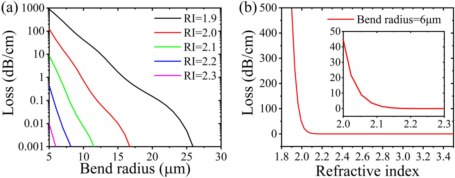
Figure 1.Calculated bend loss as a function of (a) bend radius and (b) RI of a bend waveguide with a fixed width of 3 μm and height of 460 nm. Inset in (b) is the zoom-in view of the curve. Here, the simulations are carried out at 1550 nm.
On a 460-nm-thick film deposited on a Si wafer with a 2.4-μm-thick oxidized layer as the insulator, the ultracompact MRRs with radii of 6, 10, and 15 μm are fabricated. The fabrication details are found in our previous work [29], in which the electron beam lithography (EBL) and the inductively coupled plasma (ICP) are used to pattern and etch the waveguides, with chromium (Cr) serving as the hard mask. The waveguides are finalized with air as the top cladding after residual Cr stripping.
Figures 2(a) and 2(b) show the measured transmissions of the fabricated MRRs with the ring waveguide width of 1170 nm and radii of 15 and 10 μm, respectively. Insets in the figures are scanning electron microscopy (SEM) images of the rings. A straight bus waveguide with a width of 620 nm is used to couple with each ring with a separation of 270 nm. Because higher-order modes can also be excited, we have used circles to mark the resonances of the modes on the transmission curves. By calculating the coupling efficiencies from the bus waveguide to the MRRs, i.e., 0.129–0.173 for the 15-μm-radius one and 0.117–0.16 for the 10-μm-radius one, respectively, we have determined the two MRRs to be over-coupled in the measured wavelength range from 1500 to 1600 nm. Figure 2(c) shows the SEM image of the fabricated MRR with the radius . Because it is expected to have a larger bend loss, to ensure enough light coupling, a pulley-type coupler is used to lengthen the coupling area, which has the same configuration for the waveguide widths and the separation as the point-type couplers of the large MRRs (i.e., W1 = 620, W2 = 1170 nm, gap = 270) and has a bending angle for each bend in the two s-bends. Figure 2(d) shows the measured transmission (blue line) of this MRR, and a free-spectral range (FSR) larger than 25 nm is found. Meanwhile, the coupling efficiency of the pulley-type coupler is calculated and shown as the red line in Fig. 2(d), by which one determines the coupling status at each resonance, i.e., under coupling at the resonance of 1508.171 nm and over coupling at all the other resonances [30]. Lorentzian curves are applied to fit the transmission spectrum around each resonance of all the MRRs, and Fig. 2(e) shows an example for the resonance at 1531.93 nm of the 6-μm-radius MRR. With the fittings, one can extract the intrinsic () at each resonance by using , where is the loaded , and is the transmission at the resonant wavelength. Here, the plus sign is for the under coupling, while the minus sign is for the over coupling. The extracted values of are summarized in Fig. 2(f) and distributed around (blue dashed line), (green dashed line), and (red dashed line) for the MRRs with radii of 15, 10, and 6 μm, respectively.
![]()
Figure 2.Linear measurements of the fabricated
3. POWER ENHANCEMENT FACTOR AND PURCELL FACTOR OF THE ULTRACOMPACT
As shown in Fig. 2(f), the more compact an MRR is, the lower (i.e., higher loss) it exhibits, which is usually an inevitable trade-off for a dielectric cavity. Two figures of merit (FOMs) can be applied to evaluate the overall performance of an MRR: power enhancement factor [5] and Purcell factor [31]. The former is mainly used for MRR-based nonlinear devices, and the latter can be utilized for characterizing MRR-based light source devices. The loss of a bend waveguide as a function of the bend radius generally follows the relationship [32]:
![]()
Figure 3.(a) Linear losses, (b) attainable power enhancement factors
The power enhancement factor () of an MRR is a ratio of the power in the ring () to the power in the bus waveguide () and can be expressed as follows [34]:
Here, has been used in the derivation of Eq. (3). It is clearly shown that the for an MRR is inversely proportional to both the bend waveguide loss and the cavity length. Figure 3(b) shows the calculated for MRRs with different radii based on the measured and fitted losses in Fig. 3(a). An optimal radius is found to exist where reaches the maximum. Meanwhile, when the RI increases, this optimal radius decreases, while the maximal increases. For the MRRs, the maximal is 135 at the optimal radius of 8 μm, and is 122 and 113 for the measured MRRs with radii of 10 and 6 μm, respectively.
The Purcell factor () can be calculated by [35]
4. FOUR-WAVE MIXING IN THE ULTRACOMPACT
FWM experiments in the fabricated ultracompact MRRs have been performed by using the setup illustrated in Fig. 4. The signal light and the pump light are generated from two individual continuous-wave (CW) tunable lasers, polarization tuned by fiber polarization controllers (PCs) and power adjusted by erbium-doped fiber amplifiers (EDFAs) and variable optical attenuators (VOAs). Band-pass filters are applied after the EDFAs to reduce the out-of-band amplified spontaneous emission (ASE). The two lights are combined by a 3-dB coupler, polarization selected (here is TE) by a polarization beam splitter (PBS), and then injected into the waveguides by a tapered lensed fiber. The output beam is collected by another tapered lensed fiber and measured by an optical spectral analyzer (OSA).
![]()
Figure 4.Schematic of the experimental setup for the FWM experiments in the fabricated ultra-compact
Although intermodal four-wave mixing could happen within nonresonant structures [37,38], it is indeed hard to align all the four waves to the resonances at different modes which usually exhibit different resonance spacing (i.e., the free-spectral range or FSR). Hence, here we only focus on the FWM experiments for the mode in this work despite existing resonances at other modes. For the MRRs with and , Figs. 5(a) and 5(b) show the measured output FWM spectra for on-resonances (red lines) and off-resonances (blue lines) under input pump power (i.e., power in the bus waveguide) of 13 and 16 dBm, respectively. For the MRR with , we pump it around the resonance of 1531.93 nm while 1558.72 nm for . The input signal wavelengths have one FSR separation from the pump wavelengths for both the MRRs, i.e., 1556.45 and 1543.72 nm for that with and , respectively. The input signal power is fixed to −0.81 dBm (far smaller than the pump powers) during all the measurements, while the input pump power is variable. The measured spectra show CEs of and for the MRRs with and , respectively, in which CE is defined as the ratio of the output idler power for on-resonance cases to the output signal power for off-resonance case. Here, CE represents how efficiently the MRR transfers the photon energy of the pump light to the idler light via the Kerr nonlinear process. The CEs with respect to different input pump powers are also measured and shown in Fig. 5(c). Linear fittings (red) are applied to the measured data and both show slopes of , which not only implies that the lights can be stably coupled into the MRRs, but also verifies an absent nonlinear loss of the waveguide under the current coupled powers.
![]()
Figure 5.Output FWM spectra of the ultra-compact
Figure 6(a) shows the calculated dispersions (D) of a waveguide with the width of 1170 nm and the height of 460 nm when it is straight (purple), 10-μm-radius bend (green), and 6-μm-radius bend (red), respectively. Usually, anomalous dispersions are preferred to cancel out the nonlinear phase shifts in a waveguide to achieve broadband FWM wavelength conversion [39], but the absolute values of the anomalous dispersions should not be too large. The 10-μm-radius bend waveguide exhibits anomalous dispersions with absolute values of in the wavelength range from 1575 to 1732 nm as shown in the inset of Figure 6(a). Note that if the bend is even sharper, e.g., with a radius of 6 μm, the dispersions may change to be normal. To verify the broadband operation of the fabricated 10-μm-radius MRR, we tune the signal light wavelength to be around the resonance of 1589.6 nm, i.e., two FSRs separation from the pump. Figure 6(b) shows the measured output FWM spectra for on-resonances (red) and off-resonances (blue), respectively. A CE of is achieved, only 1.5 dB degraded compared with the one-FSR separation case and suggesting a 3-dB FWM conversion bandwidth to be at least 61.8 nm.
![]()
Figure 6.(a) Calculated dispersions of straight and bend
5. DISCUSSION AND CONCLUSION
The comparison of overall performances of MRRs on different material platforms is shown in Table 2. First of all, although supercompact MRRs can be achieved in a plasmonic waveguide [18] or a Si waveguide [19], the Purcell factors are actually, not pronouncedly superior to the MRRs due to the large losses (i.e., small quality factors). Meanwhile, the extremely large loss of a plasmonic waveguide and the presence of nonlinear losses of a silicon waveguide inevitably limit their applications in nonlinear photonic devices. Among all the reported MRRs on various material platforms, the stoichiometric silicon nitride () MRRs may have the highest up to [40]. This extremely high can considerably enhance the nonlinear interactions yielding an tens of times larger than all the other MRR platforms, which finally allows for FCGs with ultralow sub-μW thresholds. However, though the also exhibits an outstanding value, it was indeed achieved in a thick (730 nm) and very wide (2.3 μm) waveguide, probably making it unsuitable for monolithic integration where a large amount of light should be decoupled into the rare-earth-doped cladding. Contrarily, light can be efficiently decoupled into the cladding of a thin (100 nm) MRR, which, however, has a super-large radius of 1.59 mm and hence a very small maximal [28]. Anyway, the MRRs were usually quite large due to a small RI of the . Recently, silicon-rich nitride (SRN) has been attracting much attention as the engineered RI can be as large as 3.1 [44,45]. Unfortunately, the high loss () of such an SRN MRR and its relatively large footprint () still give a low and .
High have been demonstrated with MRRs but they again have large radii (150 μm [42] and 136.37 μm [29]) and consequently lower and than that of the ultracompact MRRs demonstrated here. The benefits of a large are pronounced, regarding that an FWM CE of can be achieved here with a pump power of 16 dBm, while that is only for the 136.37-μm-radius MRR under the same pump power. Previously, we have achieved in a racetrack-type MRR with and straight regions being 40 μm long in total (corresponding to an effective radius of 16.37 μm of a ring-type MRR [43]), which is calculated to exhibit comparable and with the present results. Nevertheless, the bottom-up fabrication method for that MRRs may be limited by its poor scalability. Overall, compared with MRRs reported previously and MRRs in other materials, the MRRs presented here show significantly large and and the capability for scalable fabrication as well.
In conclusion, we have theoretically and experimentally investigated the way to achieve high figures of merit of an MRR. By taking advantages of the large RI of , we have demonstrated ultra-compact MRRs with the smallest radius so far, i.e., down to 6 μm. The benefits of considerably decreasing the footprints but sustaining moderately high are verified by FWM experiments, e.g., a CE of in a 10-μm-radius MRR presented here versus a CE of in a 136.37-μm-radius reported previously under the same pump powers, because the smaller one possesses a larger power enhancement factor (122 versus 15). Meanwhile, the thicker (460 nm) waveguide here can keep a small anomalous dispersion for broadband wavelength conversion, which has also been verified experimentally. Note that the loss of the 460-nm-thick waveguides shown here (5.283 dB/cmfor the straight ones) is larger than that (3.1 dB/cm) of the 360-nm-thick ones reported in our previous work [29]. It is because a longer deposition could heat the sample to a higher temperature and thus more easily allow the scattering clusters to form in the film. Apart from the losses arising from the film (i.e., absorption loss and scattering loss due to the clusters inside), the thicker waveguide may also suffer from a higher scattering loss due to the sidewall roughness. To decrease these losses and finally achieve efficient optical parametric oscillation or frequency combs in the ultracompact MRRs, both the deposition and etching processes are required to be optimized, e.g., depositing the film for several times to ensure sufficient heat dissipation to alleviate cluster formation or etching the waveguides with advanced hard mask like the hydrogen silsesquioxane (HSQ) to obtain smoother sidewalls. Besides nonlinear devices, as the ultracompact MRRs can provide large Purcell factors () as well, various light source devices may also be favored. In addition, can also be directly doped with rare-earth ions [46,47], which may further improve the emission efficiency of on-chip light sources. We believe these results shed lights on various applications which require highly efficient and ultracompact on-chip devices for the integrated photonics.
Acknowledgment
Acknowledgment. The authors thank DTU Nano-lab for the support of the fabrication facilities and technologies.
APPENDIX A
For calculating the and of MRRs demonstrated by other groups in Table?
References
[1] V. R. Almeida, C. A. Barrios, R. R. Panepucci, M. Lipson. All-optical control of light on a silicon chip. Nature, 431, 1081-1084(2004).
[2] J. Juan-Colás, A. Parkin, K. E. Dunn, M. G. Scullion, T. F. Krauss, S. D. Johnson. The electrophotonic silicon biosensor. Nat. Commun., 7, 12769(2016).
[3] M. Kues, C. Reimer, J. M. Lukens, W. J. Munro, A. M. Weiner, D. J. Moss, R. Morandotti. Quantum optical microcombs. Nat. Photonics, 13, 170-179(2019).
[4] X. Xu, M. Tan, B. Corcoran, J. Wu, A. Boes, T. G. Nguyen, S. T. Chu, B. E. Little, D. G. Hicks, R. Morandotti, A. Mitchell, D. J. Moss. 11 tops photonic convolutional accelerator for optical neural networks. Nature, 589, 44-51(2021).
[5] P. P. Absil, J. V. Hryniewicz, B. E. Little, P. S. Cho, R. A. Wilson, L. G. Joneckis, P. T. Ho. Wavelength conversion in GaAs micro-ring resonators. Opt. Lett., 25, 554-556(2000).
[6] Y. Gong, M. Makarova, S. Yerci, R. Li, M. J. Stevens, B. Baek, S. W. Nam, R. H. Hadfield, S. N. Dorenbos, V. Zwiller, J. Vučković, L. D. Negro. Linewidth narrowing and purcell enhancement in photonic crystal cavities on an Er-doped silicon nitride platform. Opt. Express, 18, 2601-2612(2010).
[7] M. Pu, L. Ottaviano, E. Semenova, K. Yvind. Efficient frequency comb generation in AlGaAs-on-insulator. Optica, 3, 823-826(2016).
[8] L. Chang, W. Xie, H. Shu, Q.-F. Yang, B. Shen, A. Boes, J. D. Peters, W. Jin, C. Xiang, S. Liu, G. Moille, S.-P. Yu, X. Wang, K. Srinivasan, S. B. Papp, K. Vahala, J. E. Bowers. Ultra-efficient frequency comb generation in AlGaAs-on-insulator microresonators. Nat. Commun., 11, 1331(2020).
[9] A. D. Bristow, N. Rotenberg, H. M. van Driel. Two-photon absorption and Kerr coefficients of silicon for 850–2200 nm. Appl. Phys. Lett., 90, 191104(2007).
[10] R. A. Soref, S. J. Emelett, W. R. Buchwald. Silicon waveguided components for the long-wave infrared region. J. Opt. A, 8, 840-848(2006).
[11] K. Ikeda, R. E. Saperstein, N. Alic, Y. Fainman. Thermal and Kerr nonlinear properties of plasma-deposited silicon nitride/silicon dioxide waveguides. Opt. Express, 16, 12987-12994(2008).
[12] J. D. B. Bradley, E. S. Hosseini. Monolithic erbium- and ytterbium-doped microring lasers on silicon chips. Opt. Express, 22, 12226-12237(2014).
[13] S. A. Miller, M. Yu, X. Ji, A. G. Griffith, J. Cardenas, A. L. Gaeta, M. Lipson. Low-loss silicon platform for broadband mid-infrared photonics. Optica, 4, 707-712(2017).
[14] M. Belt, M. L. Davenport, J. E. Bowers, D. J. Blumenthal. Ultra-low-loss Ta2O5-core/SiO2-clad planar waveguides on Si substrates. Optica, 4, 532-536(2017).
[15] X. Guan, H. Hu, L. K. Oxenløwe, L. H. Frandsen. Compact titanium dioxide waveguides with high nonlinearity at telecommunication wavelengths. Opt. Express, 26, 1055-1063(2018).
[16] E. D. Palik. Handbook of Optical Constants of Solids(1985).
[17] S. Zhu, G. Q. Lo, D. L. Kwong. Performance of ultracompact copper-capped silicon hybrid plasmonic waveguide-ring resonators at telecom wavelengths. Opt. Express, 20, 15232-15246(2012).
[18] F. Lou, L. Thylen, L. Wosinski. Experimental demonstration of silicon-based metallic whispering gallery mode disk resonators and their thermo-tuning. Optical Fiber Communications Conference, Tu2E.1(2014).
[19] Q. Xu, D. Fattal, R. G. Beausoleil. Silicon microring resonators with 1.5-μm radius. Opt. Express, 16, 4309-4315(2008).
[20] J. R. M. Osgood, N. C. Panoiu, J. I. Dadap, X. Liu, X. Chen, I.-W. Hsieh, E. Dulkeith, W. M. Green, Y. A. Vlasov. Engineering nonlinearities in nanoscale optical systems: physics and applications in dispersion-engineered silicon nanophotonic wires. Adv. Opt. Photon., 1, 162-235(2009).
[21] D. J. Moss, R. Morandotti, A. L. Gaeta, M. Lipson. New CMOS-compatible platforms based on silicon nitride and hydex for nonlinear optics. Nat. Photonics, 7, 597-607(2013).
[22] H. Jung, S.-P. Yu, D. R. Carlson, T. E. Drake, T. C. Briles, S. B. Papp. Kerr solitons with tantala ring resonators. Nonlinear Optics, NW2A.3(2019).
[23] J. Liu, E. Lucas, A. S. Raja, J. He, J. Riemensberger, R. N. Wang, M. Karpov, H. Guo, R. Bouchand, T. J. Kippenberg. Photonic microwave generation in the X- and K-band using integrated soliton microcombs. Nat. Photonics, 14, 486-491(2020).
[24] A. L. Gaeta, M. Lipson, T. J. Kippenberg. Photonic-chip-based frequency combs. Nat. Photonics, 13, 158-169(2019).
[25] L. Agazzi, J. D. B. Bradley, M. Dijkstra, F. Ay, G. Roelkens, R. Baets, K. Wörhoff, M. Pollnau. Monolithic integration of erbium-doped amplifiers with silicon-on-insulator waveguides. Opt. Express, 18, 27703-27711(2010).
[26] J. Bradley, M. Pollnau. Erbium-doped integrated waveguide amplifiers and lasers. Laser Photon. Rev., 5, 368-403(2011).
[27] G. Roelkens, L. Liu, D. Liang, R. Jones, A. Fang, B. Koch, J. Bowers. III-V/silicon photonics for on-chip and intra-chip optical interconnects. Laser Photon. Rev., 4, 751-779(2010).
[28] D. Ding, L. M. C. Pereira, J. F. Bauters, M. J. R. Heck, G. Welker, A. Vantomme, J. E. Bowers, M. J. A. de Dood, D. Bouwmeester. Multidimensional Purcell effect in an ytterbium-doped ring resonator. Nat. Photonics, 10, 385-388(2016).
[29] M. Fu, Y. Zheng, G. Li, H. Hu, M. Pu, L. K. Oxenløwe, L. H. Frandsen, X. Li, X. Guan. High-
[30] W. Bogaerts, P. De Heyn, T. Van Vaerenbergh, K. De Vos, S. Kumar Selvaraja, T. Claes, P. Dumon, P. Bienstman, D. Van Thourhout, R. Baets. Silicon microring resonators. Laser Photon. Rev., 6, 47-73(2012).
[31] E. M. Purcell. Spontaneous emission probabilities at radio frequencies. Phys. Rev., 69, 37-38(1946).
[32] M. Bahadori, M. Nikdast, S. Rumley, L. Y. Dai, N. Janosik, T. Van Vaerenbergh, A. Gazman, Q. Cheng, R. Polster, K. Bergman. Design space exploration of microring resonators in silicon photonic interconnects: impact of the ring curvature. J. Lightwave Technol., 36, 2767-2782(2018).
[33] K. Luke, A. Dutt, C. B. Poitras, M. Lipson. Overcoming Si3N4 film stress limitations for high quality factor ring resonators. Opt. Express, 21, 22829-22833(2013).
[34] M. Soltani. Novel integrated silicon nanophotonic structures using ultra-high Q resonators(2009).
[35] Y. Song, J. Wang, M. Yan, M. Qiu. Subwavelength hybrid plasmonic nanodisk with high
[36] Y. Su, P. Chang, C. Lin, A. S. Helmy. Record Purcell factors in ultracompact hybrid plasmonic ring resonators. Sci. Adv., 5, eaav1790(2019).
[37] S. Signorini, M. Mancinelli, M. Borghi, M. Bernard, M. Ghulinyan, G. Pucker, L. Pavesi. Intermodal four-wave mixing in silicon waveguides. Photon. Res., 6, 805-814(2018).
[38] C. Lacava, T. Dominguez Bucio, A. Z. Khokhar, P. Horak, Y. Jung, F. Y. Gardes, D. J. Richardson, P. Petropoulos, F. Parmigiani. Intermodal frequency generation in silicon-rich silicon nitride waveguides. Photon. Res., 7, 615-621(2019).
[39] M. Pu, H. Hu, L. Ottaviano, E. Semenova, D. Vukovic, L. K. Oxenløwe, K. Yvind. Ultra-efficient and broadband nonlinear AlGaAs-on-insulator chip for low-power optical signal processing. Laser Photon. Rev., 12, 1800111(2018).
[40] X. Ji, F. A. S. Barbosa, S. P. Roberts, A. Dutt, J. Cardenas, Y. Okawachi, A. Bryant, A. L. Gaeta, M. Lipson. Ultra-low-loss on-chip resonators with sub-milliwatt parametric oscillation threshold. Optica, 4, 619-624(2017).
[41] P. Xing, G. F. R. Chen, X. Zhao, D. K. T. Ng, M. C. Tan, D. T. H. Tan. Silicon rich nitride ring resonators for rare-earth doped telecommunications-band amplifiers pumped at the O-band. Sci. Rep., 7, 9101(2017).
[42] C. C. Evans, C. Liu, J. Suntivich. Low-loss titanium dioxide waveguides and resonators using a dielectric lift-off fabrication process. Opt. Express, 23, 11160-11169(2015).
[43] G. Li, M. Fu, Y. Zheng, X. Guan. TiO2 microring resonators with high
[44] D. T. H. Tan, K. J. A. Ooi, D. K. T. Ng. Nonlinear optics on silicon-rich nitride—a high nonlinear figure of merit CMOS platform. Photon. Res., 6, B50-B66(2018).
[45] K. J. A. Ooi, D. K. T. Ng, T. Wang, A. K. L. Chee, S. K. Ng, Q. Wang, L. K. Ang, A. M. Agarwal, L. C. Kimerling, D. T. H. Tan. Pushing the limits of CMOS optical parametric amplifiers with USRN:Si7N3 above the two-photon absorption edge. Nat. Commun., 8, 13878(2017).
[46] P. Jenouvrier, G. Boccardi, J. Fick, A. M. Jurdyc, M. Langlet. Up-conversion emission in rare earth-doped Y2Ti2O7 sol-gel thin films. J. Lumin., 113, 291-300(2005).
[47] P. Jenouvrier, M. Langlet, R. Rimet, J. Fick. Influence of crystallisation on the photoluminescence properties of Y2-

Set citation alerts for the article
Please enter your email address
© Copyright 2018-2021 | Chinese Laser Press. All Rights Reserved 沪ICP备15018463号-20