
R. B. Spielman, D. B. Reisman. On the design of magnetically insulated transmission lines for z-pinch loads[J]. Matter and Radiation at Extremes, 2019, 4(2): 27402
- Matter and Radiation at Extremes
- Vol. 4, Issue 2, 27402 (2019)
Abstract
I. INTRODUCTION
The designers of magnetically insulated transmission lines (MITLs) have traditionally used analytic approaches and simple, experimentally validated design concepts as the basis for new MITL designs. Indeed, the MITLs on the original Z machine at Sandia National Laboratories
Herein we describe an MITL design process that is more theoretically based than that used in earlier MITL designs. This MITL design process is supported by extensive theoretical and computational work on magnetic insulation by Creedon,
The key advantage of this MITL design approach is that design iterations are very fast, with typical circuit simulations taking ∼1 min on modern computers. However, it is also important to note that this approach gives physical insight into MITL design that might not be as readily apparent if the MITL design were based solely on PIC simulations.
MITL designs should have the lowest-overall-inductance MITL that has a smooth transition region between non-emissive and emissive transmission lines; they should be consistent with the thresholds for anode plasma formation resulting from electron losses; and they should have a geometry that has smooth transitions in flow impedance (vacuum impedance, gap, etc.). While we present an MITL design for a specific driver and a specific load, the approach presented herein can be readily adapted to any driver and any load.
II. ELECTRICAL SPECIFICATIONS OF THE 15-TW DRIVER
We analyzed the MITL design for the 15-TW driver described by Spielman et al.
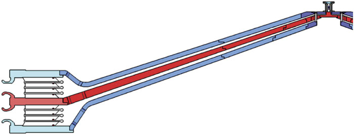
![]()
Figure 1.(a) Schematic of the full double-disk MITL that shows the insulator stack, the vacuum flare region, the MITLs, the post-hole convolute, the inner disk MITL, and the load region. (b) Schematic showing the dimensions of the two MITLs being modeled. The 1.5-Ω impedance value is only for the radius and gap at that point. The vertical scale is expanded four times for clarity.
The water transmission lines of the proposed driver can deliver a peak power up to 15 TW. The modeling described herein used the driver operating with a peak voltage of 1.25 MV in the water transmission lines at an impedance of 0.125 Ω. The resulting voltage that appears at the insulator stack is ∼1.6 MV. The peak current delivered to the load is ∼10 MA. The rise time of the current at the insulator stack is ∼100 ns. Additional electrical details can be found in Ref.
III. THE Zflow MITL MODEL
MITLs were first developed in the USA in the 1970s by researchers at Physics International Co.
We can analyze an MITL when it has an equilibrium vacuum flow condition (pressure balance). In this case, Mendel and Ottinger define the MITL performance parameters in terms of a Zflow parameter that describes the physical extent of the electron vacuum flow into the transmission line. Essentially, Zflow is the actual operating impedance of the MITL and will always be less than the geometric or vacuum impedance of the MITL because of the finite thickness of the electron sheath. Various approximations are made in the definition of the Zflow parameters. We typically design MITLs that are well insulated (even super-insulated), so the approximations described by Ottinger are valid here.
We can now define the parameters used in the Zflow MITL design process. The vacuum impedance Zvac of any portion of a transmission line is its local, geometric impedance as given by
The running impedance Zr of any segment of an MITL (or vacuum power feed) is simply the ratio of the local voltage to the local current, Zr = V/I. If any transmission line is terminated in a matched impedance, then Zvac = Zr; otherwise Zvac ≠ Zr.
The anode current Ia is the current flowing in the anode. The cathode current Ic is the current flowing in that segment of the MITL cathode. The vacuum flow current Ivac is the current flowing in the electron sheath in the vacuum in that segment of the MITL. (The difference between the anode current and the cathode current is the vacuum flow current.) The vacuum flow impedance Zflow is the impedance of that portion of the MITL gap that contains no electron flow. In the uniform-current-density limit, Zflow can be expressed as
The sheath impedance Zsh is the difference between Zvac and Zflow. The sheath impedance directly provides the sheath height hsh above the cathode. One interesting MITL figure of merit is the dimensionless ratio of the local electric field to the local magnetic field, E/cB. It is somewhat surprising that E/cB is related directly to the local running impedance Zr. A little algebra for the case of no electron flow (Ic = Ia, hsh = 0, Zflow = Zvac) gives
In the case of MITL where there is electron flow that satisfies the pressure-balance approximation of Mendel and Ottinger, the electric field in the transmission line is excluded from the electron sheath. Equation
SCREAMER simulations provide V and Ia at discrete locations in the MITL. We know the local vacuum impedance Zvac for all values of r. With this information, we can generate Zr, Zflow, hsh, Ic, Ivac, Zsh, and E/cB. We have all of the information needed to design an efficient MITL.
Ottinger et al.
From Ottinger, the minimum anode current for magnetic insulation is given bythe minimum cathode current for magnetic insulation byand the minimum value for Zflow bywhere Z0 = Zvac and Zf = Zflow. The constant fMC is given bywhere m is the electron mass, c is the speed of light, e is the electron charge, and the parameter g, g(V) = 0.995 65 − 0.053 32V + 0.0037V2, is a scale factor that is close to 1 and is generated by running many highly resolved PIC simulations.
In addition, Ottinger gave an equation for Zflow [Zf in Eqs.
IV. MITL DESIGN CRITERIA
Calculation of the Zflow parameters is a necessary but not sufficient condition to design a real-world MITL. Some of these issues were described by Stygar et al., electron losses to the anode during the setup of magnetic insulation; the transition region between non-emissive and emissive transmission lines; and transitions in MITL dimensions, shape, and impedance as a function of location.
A. Electron losses to the anode
Electrons must be lost early on during the onset of magnetic insulation. The magnitude of the loss current (density) is approximately that of Child–Langmuir space-charge-limited electron loss until B is large enough for the Larmor radius to be less than about one-half the local MITL gap h. The electron losses scale as h−2 and V3/2, and larger anode–cathode (AK) gaps have smaller electron losses to the anode. Consequently, we do not have arbitrary flexibility to choose a small-gap (low-impedance) MITL, even if that MITL satisfied the Zflow design criteria, since, eventually, sufficient electrons will be lost to the anode to heat the anode above the empirically determined ∼400 °C threshold for desorption of hydrogen from the anode and create an anode plasma.
B. Transition region to magnetic insulation
Any real pulsed-power vacuum feed has a transition from the permanently non-emissive region near the insulator stack to a full-fledged MITL [shown in
C. MITL transitions
Once magnetic insulation is established, changes to the key Zflow MITL parameters radially along the MITL should be gradual. Extensive data from Sandia’s Z machine showed that vacuum insulation remains very good, even though there are slow changes to the MITL Zvac over ∼10 cm of radius. Empirically then, we can restate this slow transition rule as: The Zflow MITL parameters (Zflow, Ivac, hsh) must all have small, gradual changes over the region of transition. Simulations by Pointon et al.
The Zflow MITL parameters such as Zflow, Ivac, hsh, and E/cB depend on the local MITL impedance. Qualitatively, decreases in MITL gap (decreases in impedance) will decrease Zflow and increase Ivac, hsh, and E/cB. The designer must be cautious whenever the local Zflow approaches one-half Zvac and when E/cB ∼ 1.0. In fact, there are cases with Zflow higher than one-half Zvac that are not well insulated.
V. A CONSTANT-IMPEDANCE MITL DESIGN FOR z-PINCH LOADS
The simplest approach to disk MITL design is to use a constant-impedance disk MITL until one is near the PHC. This design is shown schematically in
The simple case for an MITL of a constant vacuum impedance Zvac terminated in a matched impedance is a vacuum feed having a constant voltage and constant current along the MITL. This means that Zr = Zflow and Zflow is constant along the MITL, and therefore E/cB is also constant in the MITL. The current in the vacuum electron flow, Ivac, is constant along the MITL. The electron sheath height hsh, as a fraction of the MITL gap, is constant (shrinking in absolute terms).
The case of an MITL of a constant vacuum impedance Zvac terminated in an impedance lower than the vacuum impedance is interesting. In this case, we have a vacuum feed with a constant voltage and constant current along the MITL, but we find that Zflow ≠ Zr. Any termination impedance that is lower than Zvac gives a Zr that is lower than Zvac. Again, Zflow is constant along the MITL and, therefore, E/cB is also constant in the MITL, but in this case E/cB is lower than the matched case. The electron current in the vacuum electron flow Ivac is constant along the MITL but lower than in the matched case. The actual electron sheath hsh as a fraction of the MITL gap is constant but smaller than in the matched case.
In reality, the MITLs driving a dynamic z-pinch load are essentially driving a purely reactive short-circuit load. Until peak current (∼100 ns), the total circuit inductance is nearly constant. This means that the MITL is terminated in a short circuit with an effective inductance in series with the MITL. We describe such a load as very undermatched. In our case, the length of the MITL is short compared with the pulse length, so the entire MITL is load-dominated at all times. Very undermatched loads have the effect of lowering the voltage on the MITL by up to a factor of 2 and increasing the current by up to a factor of 2 over the matched case. It is easy to see that E/cB decreases by up to four times as well. This is a very good thing for magnetic insulation. Another qualitative consequence of this sort of undermatched load is that Zr decreases radially inward and decreases in time after peak voltage and before peak current. This is translated directly to E/cB decreasing in radius and time (after peak MITL voltage).
We model idealized disk MITLs that extend from the region near the insulator stack to the constant-gap MITL section at a radius of 30 cm. The initial height of the vacuum feed at a radius of 155 cm is 11.43 cm.
The inductance of a 2-Ω MITL with a length of 4.038 ns is 8.076 nH by inspection. The total inductance of the vacuum feed and load in these calculations is 10.56 nH. This inductance is the paralleled inductance of the A- and B-level feeds, the PHC, the disk MITL, and the load.
A. SCREAMER simulation of a 2-Ω MITL
We now describe the results of SCREAMER
A SCREAMER calculation for our driver using 2-Ω constant-impedance MITLs and a Z51 wire-array z-pinch load gives us detailed voltage, current, and MITL information in time. The overall current performance is shown in
![]()
Figure 2.Calculated total current (black solid curve), A-level current (red solid curve), and B-level current (blue solid curve) as functions of time.
The detailed current profiles at the ten MITL locations in the B-level MITL are shown in
![]()
Figure 3.Calculated currents in each MITL segment as functions of time. The differences seen in the time window from 120 ns to 140 ns reflect losses during the setup of magnetic insulation.
In
![]()
Figure 4.Calculated voltages in each MITL segment as functions of time.
| MITL segment | Radial location (cm) | AK gap (cm) | Zvac (Ω) | Va (MV) | Ec (kV/cm) | Ia (MA) | Zr (Ω) | Zflow (Ω) | Ic (MA) | Ivac (kA) | E/cB | hsh (mm) | hsh/gap |
|---|---|---|---|---|---|---|---|---|---|---|---|---|---|
| 1 | 144.95 | 4.835 | 2 | 1.28 | 265 | 2.77 | 0.462 | 1.978 | 2.693 | 77 | 0.234 | 0.52 | 0.0108 |
| 2 | 132.85 | 4.431 | 2 | 1.22 | 275 | 2.77 | 0.440 | 1.980 | 2.701 | 69 | 0.223 | 0.45 | 0.0101 |
| 3 | 120.75 | 4.028 | 2 | 1.17 | 290 | 2.77 | 0.422 | 1.980 | 2.706 | 64 | 0.213 | 0.40 | 0.0099 |
| 4 | 108.65 | 3.624 | 2 | 1.12 | 309 | 2.77 | 0.404 | 1.981 | 2.712 | 58 | 0.204 | 0.34 | 0.0094 |
| 5 | 96.55 | 3.220 | 2 | 1.07 | 332 | 2.77 | 0.386 | 1.982 | 2.717 | 53 | 0.195 | 0.29 | 0.0088 |
| 6 | 84.45 | 2.817 | 2 | 1.01 | 359 | 2.77 | 0.365 | 1.983 | 2.723 | 47 | 0.184 | 0.24 | 0.0083 |
| 7 | 72.35 | 2.413 | 2 | 0.966 | 382 | 2.77 | 0.349 | 1.984 | 2.727 | 43 | 0.176 | 0.19 | 0.0080 |
| 8 | 60.25 | 2.010 | 2 | 0.906 | 451 | 2.77 | 0.327 | 1.985 | 2.732 | 38 | 0.165 | 0.15 | 0.0075 |
| 9 | 48.15 | 1.606 | 2 | 0.855 | 532 | 2.77 | 0.309 | 1.986 | 2.736 | 34 | 0.155 | 0.11 | 0.0071 |
| 10 | 36.05 | 1.202 | 2 | 0.803 | 668 | 2.77 | 0.290 | 1.986 | 2.740 | 30 | 0.146 | 0.08 | 0.0068 |
Table 1. Listing of the MITL parameters from the ten MITL segments on the B level from SCREAMER calculations for a 2-Ω constant-impedance MITL.
Several items of interest can be seen in Note that the Zr decreases strongly with decreasing radius. It will eventually approach the driving impedance of 0.25 Ω. This is caused by the reduction in local voltage with radius. This voltage drives the ratio E/cB, which decreases strongly with decreasing radius. This means that the “quality factor” for magnetic insulation is slowly increasing with decreasing radius. This is very good. The flow impedance Zflow increases very weakly with decreasing MITL radius. (Zflow cannot be larger than Zvac, so the difference between Zvac and Zflow is getting smaller.) This implies that the quality of magnetic insulation is slowly improving with decreasing radius. The cathode current (directly from Zflow) increases with decreasing radius. This means that the fraction of the current in the vacuum electron flow is decreasing with decreasing radius. Again, this means that magnetic insulation is improving with decreasing radius. The amount of current in the vacuum electron flow is trivial compared with the total B-level current. The size of the electron sheath, hsh, decreases with decreasing radius as driven by Zflow. This is true even as a fraction of the gap. The electron sheath is remarkably thin (a fraction of a millimeter). This is very good for magnetic insulation. Since these electrical parameters are taken at peak MITL voltage with a rising current, all of the magnetic-insulation Zflow parameters discussed above improve later in time until peak current (voltage falls and current increases). The peak value of the electric field (at 175 ns) increases radially inward. Early in time, this means that the cathode of the innermost MITL segment (segment 10) will start emitting electrons (self-limited) before any of the other MITL segments, because its electric field will exceed the electron-emission threshold first. As the applied voltage continues to increase, after the start of electron emission from MITL segment 10, MITL segments at larger radii start to emit electrons. One can think of the emission front moving outward, not inward as is presented in many papers.
At peak voltage, the 2-Ω MITL is becoming more safely insulated with decreasing radius. The calculated reduction in the vacuum-electron-flow current means that electron retrapping is taking place. The fraction of the current in vacuum flow is insignificant even at peak voltage and, even if all of that vacuum-electron-flow current is lost at the PHC, it is not a significant current loss. [Note that the magnitude of electron losses at the PHC depends on the convolute voltage, and those losses increase dramatically with peak driver current (PHC voltage), as was seen going from Z to ZR.] These MITL behaviors are typical with z-pinch loads that are effectively a short circuit until peak current, after which the dL/dt voltage makes magnetic insulation more perilous. This type of MITL is referred to as a super-insulated MITL by Ottinger et al.
We plot the electron-loss current to the anode in the B-level MITL segments in
![]()
Figure 5.Electron-loss currents in each MITL segment, where the largest current losses occur with the inner MITL segment 10.
![]()
Figure 6.Electron-loss current density in each MITL segment, where the largest current density losses occur with the inner MITL segment 10.
The electron-loss current density plot of
The detailed anode deposition energy and anode temperature rise, caused by these electron losses, need quantitative results from a high-resolution PIC simulation with electron-energy deposition in the anode and anode heating (ITS Tiger post processor
We conclude that a 2-Ω constant-impedance MITL will have minimal electron losses during the setup of magnetic insulation in the outer disk MITL and measurable losses in the inner disk MITL (still lower than the losses on the working Sandia Z-machine MITLs). The quality of the magnetic insulation at peak MITL voltage is very good, and the magnetic insulation quality is increasing with decreasing radius and increasing time. This 2-Ω vacuum feed is a very safe, first-cut MITL design—just as the vacuum feed was on the Z machine. The MITL design will work well for the 15-TW driver that we are modeling. Again, the fact that the electron-loss current density is much lower at larger radii than at smaller radii suggests that improvements in the MITL design, lowering inductance, can be made.
VI. A VARIABLE-IMPEDANCE MITL DESIGN FOR z-PINCH LOADS
What can we do to improve the coupling efficiency of the driver to the load? The energy-coupling efficiency to a z-pinch load improves with decreasing total inductance until L ∼ 0.8 Z t, where Z is the impedance of the driver and t is the rise time of the current. For our proposed driver and load, that means that the optimum total inductance is ∼10 nH. The total inductance of the constant-impedance MITL design above with a Z51 load is ∼10.6 nH. (Note that the Z51 load is one of the lowest-inductance dynamic loads that would be fielded, and other loads would have a higher initial inductance.) We can therefore increase overall coupling efficiency if we can slightly lower the MITL inductance. We can decrease the inductance (gap) of the feed, but we need to monitor all of the Zflow parameters of the MITL. Do we have a 2D EM PIC code justification for these arbitrary MITL geometry changes? Yes, because the Zflow model has been benchmarked by Ottinger et al.
Consider that the outer MITL segments of the 2-Ω MITL have electron-loss current densities nearly 1000 times lower than the “maximum acceptable” electron-loss current density found in the inner MITL segments. We propose a variable-impedance MITL with an outer MITL impedance of 1.5 Ω and an inner MITL impedance of 2 Ω. There are no other changes to the simulation from the constant-impedance MITL case. We address the radial disparity in loss current density by decreasing the gap (decreasing the impedance and increasing the loss current) at the large-radius (outer) entrance to the variable-impedance MITL. The variable-impedance MITL is then composed of a smoothly varying impedance (geometric straight line) to the unchanged inner segment of the variable-impedance MITL. As before, we divide the variable-impedance MITL into ten segments of 0.4010-ns length each. The variable-impedance MITL profile and other information are shown in
| MITL segment | Radius centroid (cm) | Circular centroid (cm) | Calculated gap (cm) | Local impedance (Ω) | Local inductance (H) (×10−10) |
|---|---|---|---|---|---|
| 1 | 144.2565 | 906.4 | 3.621 | 1.505 | 6.0384 |
| 2 | 132.2295 | 830.8 | 3.345 | 1.517 | 6.0858 |
| 3 | 120.2025 | 755.3 | 3.070 | 1.531 | 6.1427 |
| 4 | 108.1755 | 679.7 | 2.794 | 1.549 | 6.2122 |
| 5 | 96.1485 | 604.1 | 2.518 | 1.570 | 6.2991 |
| 6 | 84.1215 | 528.6 | 2.242 | 1.598 | 6.4109 |
| 7 | 72.0945 | 453.0 | 1.966 | 1.635 | 6.5600 |
| 8 | 60.0675 | 377.4 | 1.690 | 1.687 | 6.7689 |
| 9 | 48.0405 | 301.8 | 1.414 | 1.765 | 7.0822 |
| 10 | 36.0135 | 226.3 | 1.139 | 1.896 | 7.6049 |
Table 2. Radius, circumference, gap, impedance, and inductance of the ten MITL segments used in the SCREAMER calculations.
We model the idealized variable-impedance disk MITL that extends from the region near the insulator stack to the constant-gap MITL section at a radius of 30 cm. The initial height of the vacuum feed at a radius of 155 cm is unchanged at 11.43 cm.
We expect that this change in MITL profile will leave the electron losses on the inner MITL segment nearly unchanged while increasing the electron losses in the outer MITL segments. The largest percentage increase in electron losses will be at the outermost segment of the MITL, which has the largest absolute decrease in gap. The change to a variable-impedance (1.5-Ω to 2.0-Ω) MITL results in a lowering of the disk MITL inductances to ∼6.52 nH each (from 8.07 nH each for the 2-Ω case). The total geometric inductance of the vacuum feed decreases from 10.56 nH to 9.8 nH. (This inductance is the paralleled inductance of the A- and B-level feeds, the PHC, the disk MITL, and the Z51 load.)
A. SCREAMER simulation of a 1.5-Ω to 2.0-Ω variable-impedance MITL
A SCREAMER calculation for the 15-TW driver using 1.5-Ω to 2-Ω variable-impedance MITLs and a z-pinch load gives us detailed voltage, current, and MITL information in time and space. The overall current performance is shown in
![]()
Figure 7.Calculated total current (black solid curve), A-level current (red solid curve), and B-level current (blue solid curve) as functions of time.
The B-level MITL current information in
![]()
Figure 8.Calculated currents in each MITL segment as functions of time for the variable-impedance MITL. The differences in the various currents seen at ∼120 ns to 150 ns reflect losses during the setup of magnetic insulation.
In
![]()
Figure 9.Calculated voltages of each MITL segment with time. The voltages decrease radially inward.
| MITL segment | Radial location (cm) | AK gap (cm) | Zvac (Ω) | Va (MV) | Ec (kV/cm) | Ia (MA) | Zr (Ω) | Zflow (Ω) | Ic (MA) | Ivac (kA) | E/cB | hsh (mm) | hsh/gap |
|---|---|---|---|---|---|---|---|---|---|---|---|---|---|
| 1 | 144.95 | 3.639 | 1.505 | 1.231 | 338 | 2.92 | 0.422 | 1.479 | 2.799 | 121 | 0.285 | 0.62 | 0.0171 |
| 2 | 132.85 | 3.361 | 1.517 | 1.188 | 353 | 2.92 | 0.407 | 1.493 | 2.809 | 111 | 0.273 | 0.54 | 0.0160 |
| 3 | 120.75 | 3.083 | 1.531 | 1.145 | 371 | 2.92 | 0.392 | 1.508 | 2.820 | 101 | 0.260 | 0.47 | 0.0151 |
| 4 | 108.65 | 2.806 | 1.548 | 1.103 | 393 | 2.92 | 0.378 | 1.530 | 2.829 | 91 | 0.248 | 0.40 | 0.0142 |
| 5 | 96.55 | 2.528 | 1.570 | 1.060 | 419 | 2.92 | 0.363 | 1.549 | 2.840 | 81 | 0.234 | 0.33 | 0.0131 |
| 6 | 84.45 | 2.250 | 1.598 | 1.017 | 452 | 2.92 | 0.348 | 1.579 | 2.850 | 72 | 0.221 | 0.27 | 0.0121 |
| 7 | 72.35 | 1.973 | 1.635 | 0.966 | 490 | 2.92 | 0.331 | 1.617 | 2.858 | 62 | 0.205 | 0.22 | 0.0110 |
| 8 | 60.25 | 1.695 | 1.687 | 0.923 | 545 | 2.92 | 0.316 | 1.671 | 2.867 | 53 | 0.189 | 0.17 | 0.0098 |
| 9 | 48.15 | 1.417 | 1.765 | 0.880 | 621 | 2.92 | 0.301 | 1.750 | 2.876 | 44 | 0.172 | 0.12 | 0.0085 |
| 10 | 36.05 | 1.140 | 1.895 | 0.829 | 727 | 2.92 | 0.284 | 1.882 | 2.887 | 33 | 0.151 | 0.08 | 0.0070 |
Table 3. Listing of B-level MITL parameters from SCREAMER calculations for a variable-impedance MITL.
Several items of interest are seen in With this variable MITL impedance, the flow impedance Zflow increases smoothly with decreasing MITL radius. In all of the segments of the MITL, Zflow is capped by the local MITL vacuum impedance. The cathode current increases with decreasing radius (or, equivalently, the vacuum electron flow decreases with decreasing radius). The absolute values of the cathode current are higher than in the 2-Ω MITL case. The magnitude of the vacuum current is higher for MITL segment 1 in the variable-impedance MITL than in the 2-Ω MITL, but by the time MITL segment 10 is reached, the vacuum currents are almost identical. The smaller gap in MITL segment 1 (higher E) is the cause of the increased vacuum current. The running impedance is lower for all MITL segments in the variable-impedance MITL case than for the same segments in the 2-Ω MITL case. The ratio E/cB continues to decrease strongly with decreasing radius. The value of E/cB starts larger because of the smaller gaps (lower impedance and higher electric field) at larger radii, but ends up nearly the same at the inner radii as the 2-Ω results in The size of the electron sheath starts larger than in the 2-Ω case, but decreases rapidly with decreasing radius. The sheath size at the inner edge of the MITL is similar to the 2-Ω case shown in
The SCREAMER calculations show that the variable-impedance MITL continues to be robustly insulated with decreasing radius. The reduction in the vacuum-electron-flow current means that electron retrapping is taking place. The fraction of the current in vacuum flow at peak voltage remains small. While the sheath size and vacuum current are higher in MITL segment 1 than in 2-Ω MITL segment 1, they are nearly the same as those of the 2-Ω MITL in MITL segment 10.
The current losses in each segment of the variable-impedance MITL continue to show that the lowest electron-loss current is on the outer MITL segments (largest gap), with increasing loss current densities on the inner MITL segments (see
![]()
Figure 10.Electron-loss currents in each MITL segment for the variable-impedance MITL, where the largest current losses occur with inner MITL segment 10.
![]()
Figure 11.Electron-loss current density in each MITL segment of the variable-impedance MITL, where the largest current-density losses occur with inner MITL segment 10.
Examination of the values of the electron-loss current density in each segment of the variable-impedance MITL shows that the lowest electron-loss current density remains in the outer MITL segments (largest gap), with increasing loss current densities in the inner MITL segments (see
The variable-impedance MITL design shown here (1.5 Ω to 2 Ω) is not intended to be the best or final design. It is only indicative of the improvements that can be made in overall MITL inductance while maintaining robust and safe magnetic insulation. These designs do not address design refinements such as a gradual impedance taper at the radius where the variable-impedance MITL meets the constant-gap MITL, nor do they take into account the transition in the vacuum flare profile to the outer MITL.
We note that Pointon and Savage
VII. DISCUSSION
The electron losses seen at each MITL segment are a strong function of local impedance (gap) and local electric field. The differences in electron-loss current density are driven, first, by the higher electric fields seen on the inner MITL segments and, second, by the differences in the surface areas of the inner MITL segments versus the outer MITL segments. We see that the losses in the inner MITL segment for both MITL cases are much higher than those in the outer MITL segments. This suggests, on the one hand, that further decreases in the impedance at the outer MITL radius will lower total inductance. On the other hand, assembly tolerances of the MITLs, debris on the MITLs, and defects in their surfaces could cause MITL electron-loss current densities in excess of the calculated values. A careful comparison of the reliability risks of lower-inductance MITLs versus the benefits of better coupling to the load needs to be made.
Further decreases in MITL impedances (gaps) at the outer MITL radius could increase MITL losses in the outer MITL segments compared with higher-impedance MITL designs (1.5 Ω and 2 Ω). However, the total inductance gains with decreasing outer MITL impedance will be proportionally smaller owing to the irreducible inductances in other parts of the circuit (the insulator stack, the PHC, the inner disk feed, and the load). Even in our two cases, a reduction in the inductance of each disk MITL by 1.56 nH (from 8.075 nH in the 2-Ω case to 6.52 nH in the 1.5-Ω to 2-Ω case) only reduced the total inductance of the system by 0.76 nH (the final inductance is effectively the inductance reduction of two MITLs in parallel) from 10.56 nH to 9.8 nH. Further gains in total inductance will begin to asymptote with continued reductions in outer MITL impedance. For example, for Zouter = 1.0 Ω (2.51-cm AK gap) and Zinner = 2.0 Ω, the total inductance is lowered to 9.05 nH. It is unfortunate that the cost (and time) invested in building large-diameter MITLs leads to very conservative design decisions and precludes a thorough experimental study of riskier but more efficient MITL designs.
VIII. CONCLUSION
We have shown two different MITL designs, based on the Zflow MITL model, that were developed with the SCREAMER circuit code. The 2-Ω constant-impedance MITL is very similar to the well-tested Z-machine MITLs, and the variable-impedance (1.5-Ω to 2-Ω) MITL is one possible improvement in MITL inductance and overall driver coupling efficiency. Both designs have robust magnetic insulation as suggested by the Zflow model used in SCREAMER. Validation of vacuum power flow with highly resolved PIC codes is always required for actual designs. We have shown that we can design MITLs using SCREAMER for the case of a z-pinch load but suggest that the same design philosophy can be used with arbitrary drivers and loads.
References
[9] M. E. Savage, T. D. Pointon. 2-D PIC simulations of electron flow in the magnetically insulated transmission lines of Z and ZR, 151(2005).
[10] M. E. Savage, T. D. Pointon, W. L. Langston. Computer simulations of the magnetically insulated transmission lines and post-hole convolute of ZR, 165(2007).
[12] J. M. Creedon. Magnetic cutoff in high‐current diodes. J. Appl. Phys., 48, 1070(1977).
[20] M. S. Di Capua. Magnetic insulation. IEEE Trans. Plasma Sci., 11, 205(1983).
[25] C. W. Mendel, . Status of magnetically-insulated power transmission theory(1995).
[32] J. W. Schumer, D. D. Hinshelwood, R. J. Allen, P. F. Ottinger, R. D. Curry. Benchingmark and implementation of a generalized MITL flow model, 1176(2009).
[34] R. B. Spielman, Y. Gryazin. SCREAMER v4.0—A powerful circuit analysis code(2015).

Set citation alerts for the article
Please enter your email address
© Copyright 2018-2021 | Chinese Laser Press. All Rights Reserved 沪ICP备15018463号-20