
Yu Fan, Qianqian Yuan, Haitao Jiang. Fabrication of low Mg content MgxZn1-xO nanowires ultraviolet photosensors via chemical vapour deposition method[J]. Infrared and Laser Engineering, 2021, 50(9): 20200448
- Infrared and Laser Engineering
- Vol. 50, Issue 9, 20200448 (2021)
Abstract
0 Introduction
Over the past decade, one-dimensional nanostructures, including nanowires(NW), nanorods, nanotubes and nanobelts, with various compositions and morphology have been fabricated by many approaches[
In this paper, MgZnO NWs have been successfully fabricated via CVD using the mixture of the zinc oxide powder and commerical graphite poweder and Mg powder as the precursor material without any catalysts. The advantages of this method include facile and catalyst-free growth of MgxZn1-xO NWs on SiO2/Si substrate and the subsequent transfer-free fabrication of electronic or optoelectronic devices.
1 Experiment
1.1 Pretreatment of the substrate
The SiO2/Si wafer was cleaned with acetone, ethanol and deionized water in turn under the ultrasound, and then the wafer was dried with a compressed nitrogen. The substrate is heated for 2 min at 100 ℃ being coated with AZ3100 photoresist in a spin coater at 3500 r/min. Then, the periodical square pillar microstructure with a top area size of 10 mm × 10 mm and a height of around 800 nm was fabricated on substrate surfaces by RIE(Magnetic Enhanced Reactive Ion Etching, SF6∶CHF3 = 10∶40) after a UV lithography process.
1.2 Preparation of MgZnO nanowires
The growth of MgxZn1-xO nanowires was performed in a horizontal tube furnace. This system contained a quartz tube vacuum chamber 100 cm long and 10 cm in diameter. A smaller one-ended quartz tube, 50 cm long, and 2 cm in diameter that contained precursor materials(ZnO and Mg) and substrate was placed into the vacuum chamber. A mixture of the zinc oxide powder(99.99%) and commercial graphite powder(weight ratio 1∶1) was used as the precursor material of fabricating ZnO, and Mg powder(99.99%) was also used as the doped material. The precursor material of ZnO was placed at the quartz coat, and the SiO2/Si substrate was placed over the quartz coat, while the Mg powder was placed at the closed end of the smaller quartz tube. Then the smaller quartz tube was inserted into the the center of the low-temperature region of the quartz tube vacuum chamber, and the quartz coat was inserted into at the center of the high-temperature region of the quartz tube vacuum chamber.
A mixture of the zinc oxide powder(99.99%) and commercial graphite powder(weight ratio 1∶1) was used as the precursor material of fabricating ZnO, and Mg powder(99.99%) was also used as the doped material. The precursor material of ZnO was placed at the quartz coat, and the SiO2/Si substrate was placed over the quartz coat, while the Mg powder was placed at the closed end of the smaller quartz tube. Then the smaller quartz tube was inserted into the the center of the low-temperature region of the quartz tube vacuum chamber, and the quartz coat was inserted into at the center of the high-temperature region of the quartz tube vacuum chamber.
The precursor material of ZnO and Mg were heated up to 1000 ℃ and 760 ℃, respectively, and the temperature was maintained about 30 minutes during the growth process of the MgxZn1-xO nanowires, and the high purity Ar gas, as carrier gas, was fed into the furnace at one end at the rate of 100 sccm, while the other end was connected to rotary pump to keep the system to a certain pressure. When the temperature was heated to the designed temperature, the high purity O2 gas was introduced into the quartz tude at the rate of 2 sccm. After the chamber cooled down to the room temperature, the white materials appeared on the substrates.
2 Results and discussion
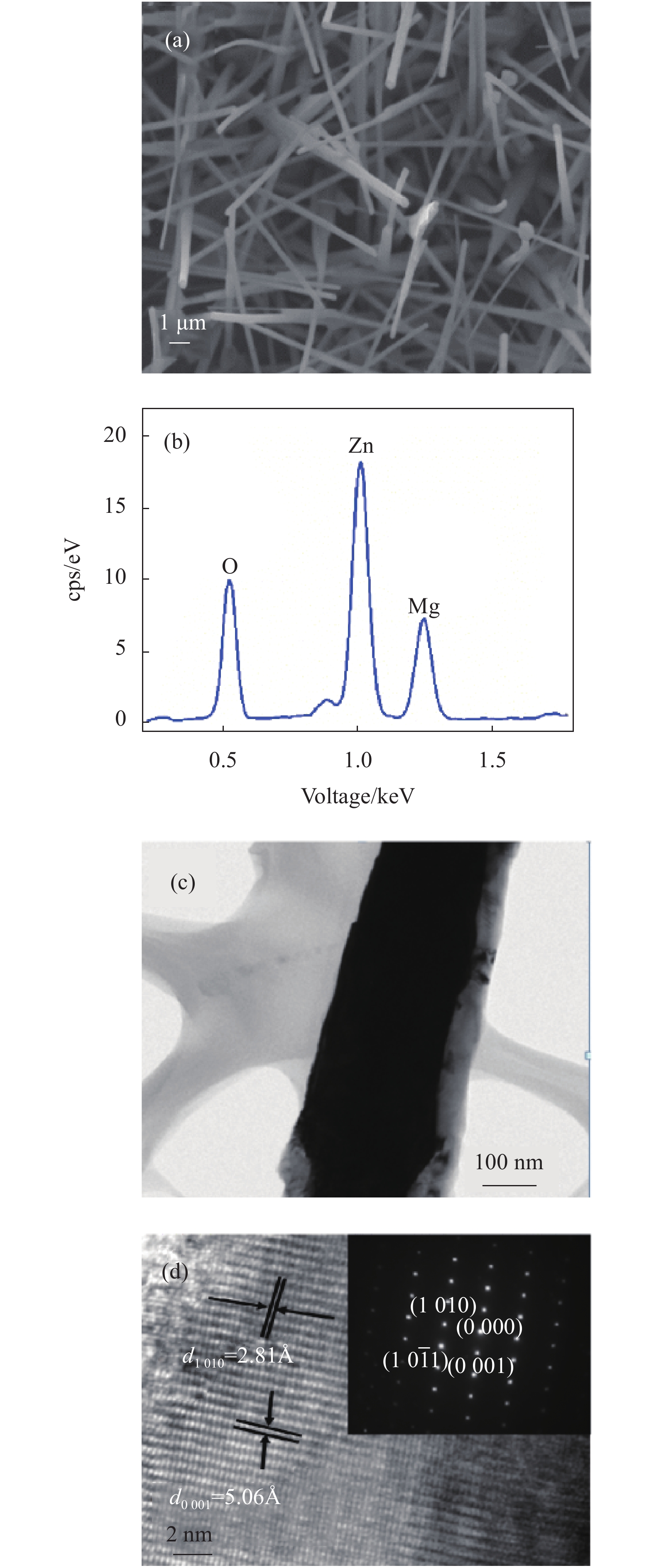
SEM was used to characterize the morphology of the products. Figure 1 shows the SEM of the MgZnO NWs. Figure 1(a) and Figure 1(b) showed the top-view SEM images of the MgZnO NWs and EDS, respectively. From the Figure 1(b), it was clear that only the Zn, Mg and O peaks were observed while no other impurities were detected. Figure 1(c) showed the image of sample used for TEM. Figure 1(d) revealed that structure of the MgZnOnanowire was hexagonal structure(PDF#36-1451), the lattice parameter was 2.81 Å(1 Å=0.1 nm), 5.06 Å, respectively, which meaned the Mg ions started to replace the Zn ions. Meanwhile, the corresponding chemical composition of the grown MgZnO NWs was determined through the EDS.
![]()
Figure 1.(a) Top-view SEM images of the as-grown MgZnO NWs; (b) EDS image of MgZnO NWs; (c) Single morphology of MgZnO NW sample for TEM; (d) High resolution TEM of the MgZnO nanowire, insert images show the corresponding SAED pattern, respectively
In order to further confirm the formation of MgZnO NWs, the X-ray diffraction(XRD) and Photo-luminescence(PL) of ZnO NWs and MgZnO NWs were checked, showed in Figure 2. XRD patterns of NWs samples were taken to study the crystallographic information on the nanowires. From the diffraction peaks shown in Figure 2(a), it could deduce that the structure of MgZnO NWs was hexagonal, just like ZnO. Meanwhile, the normalized PL spectra of the MgZnO samples are shown in Figure 2(b), the PL spectra showed an obvious peak at the 378 nm. Comparing with the ZnO PL, the MgZnO showed an apparent hypsochromic shift, which was caused by the change of the band-gap with Mg substitution. Owing to Mg doping the ZnO nanowires, the Burstein-Moss effect is deemed to be the reason of the hypsochromic-shift.
![]()
Figure 2.(a) XRD of the ZnO nanowires and MgZnO nanowire; (b) PL spectrum of the ZnO nanowires and MgZnO nanowire. The PL shows the peak of MgZnO blue shift
Current-voltage(I-V) measurements were carried out at ambient condition to investigate the electrical properties of the fabricated UV photosensor in dark and under UV illumination. Metal electrodes could be directly fabricated through screen printing or shadow-mask assisted deposition method onto the as-obtained MgZnO nanowires.
In our experiment, silver paint was directly applied onto MgZnO nanowire arrys to form the electrods. The photoresponse tests were conducted in a dark environment with UV illumination (254 nm, 0.03 mW/cm2). The "on" and "off" of illumination were controlled by a metal chopper. The photoresponse of UV illumination are shown in Figure 3. Figure 3(b) shows the I-T characteristic curves of MgZnO nanowires photodetector with and without light illumination.
![]()
Figure 3.
To further analyze the photoconductive properties, the chemical states of NWs surface with and without UV radiation can be clarified based on the previous findings. Under dark conditions, the surface of MgZnO NWs absorbed oxygen from the atmosphere and formed a depletion layer, thereby producing negatively charged ions. As a result, the absorbed oxygen molecules on the surface of the MgZnO NWs trapped some of the free electrons, whereas the mobility of the remaining electrons decreased because of the depletion layers created on the surface.
The water vapor molecules absorbed by the surface of MgZnO NWs also enhanced the depletion layer. The water vapor molecules captured not only free electrons but also free holes, thereby further lowering the conductivity NWs. Consequently, H2O molecules significantly affected the conductivity more than O2 molecules in MgZnO NWs.
Electron-hole pairs were generated (
The response time is another important indicator of merit of a photodetector. To examine the response time of the MgZnO nanowires UV photodetector, the time-dependent photo-current at 3 V bias with multiple UV on/off cycles was measured, in which both the "on" and "off" times of the UV illumination were 20 s. It was well-known oxygen molecules absorbed at surface of MgZnO acting as electron acceptors to form O2 by capturing free electrons from the surface of MgZnO in dark and created a low conductive depletion layer near the surface of nanowires.
Upon UV illumination, the photogenerated holes in MgZnO migrated to the surface and neutralized the O2 ions, while the unpaired electrons significantly enhanced the conductivity of the sample. As shown in Figure 3(b), upon UV illumination, the current would first rapidly ramp from the dark current, followed by a slow increase; and as UV illumination was off, the current would first promptly fall, and then slowly decay to around the original level. These observed time-resolved photocurrent course could be described by a fast photoresponse process followed by a slow one, and the latter one was governed by the low rate of the turnover of oxygen chemisorption/desorption on the NWs surface. The dependence of both rose and decay of photocurrent on time could be well described by second-order decay functions as follows:
Where, I0, A, and B are constants, t1 and t2 are time constants.
Figure 3(c) and Figure 3(d) showed a typical rise and decay stage of the time-resolved photocurrent variation curve, respectively. By fitting the photocurrent data with the time, it was estimated the time constants for rise stage are tr1 = 0.47 s, tr2 = 3.99 s, with relative weight factors of 64% and 36% respectively; while the time constants for decay stage are td1 = 0.60 s, td2 = 2.01 s, with relative weight factors of 40% and 60%, respectively.
It was expected that the performance of our MgZnO nanowire photodetectors could be further improved by employing thermal annealing, plasmonic nanoparticles modifica-tion, heterojunction creation, and so on. For the rise stage, the fast process was a result of photocarriers generation excited by UV illumination, however, the slow one was governed by readsorption of oxygen molecules on MgZnO surface; when the UV illumination was off, the fast decay process was related to photocarrier recombination, and the slow one was controlled by the slow physisorption of oxygen molecules.
3 Conclusions
In summary, it was demonstrated that the MgZnO nanowire arrays could be grown on SiO2/Si substrate using the CVD without predeposited catalyst or seed-layer. The advantages of this method include facile and safe achievement of the growth of MgZnO nanowires on SiO2/Si substrate; and the Mg content of MgZnO could be adjusted by changing the ratio of the source materials and the subsequent transfer-free fabrication of electronic or optoelectronic devices. The PL spectra of the MgZnO samples show abvious blue-shift. The MgZnO nanowire UV photodetector was fabricated by a transfer-free process presented high responsibility performance. The strategy shown here would greatly reduce the complexity in nanodevice fabrication processes and significantly prompt the application of MgZnO nanostructures in nano-electronics and optoelectronics.
References
[1] Y Li, F Qian, J Xiang, et al. Nanowire electronic and optoelectronic devices. Mater Today, 9, 18-27(2006).
[2] C M Lieber, Z L Wang. Functional nanowires. MRS Bull, 32(2), 99-108(2007).
[3] Z L Wang. ZnO nanowire and nanobelt platform for nanotechnology. Mater Sci Eng R, 64(3-4), 33-71(2009).
[4] R M Yu, C F Pan, Y F Hu, et al. Enhanced performance of GaN nanobelt-based photodetectors by means of piezotronic effects. Nano Res, 6(10), 758-766(2013).
[5] B Liang, H T Huang, Z Liu, et al. Ladder-like metal oxide nanowires Synthesis, electrical transport, and enhanced light absorption properties. Nano Res, 7(2), 272-283(2014).
[6] Y Xia, P Yang, Y Sun, et al. One-dimensional nanostructures: Synthesis, characterization, and applications. Adv Mater, 15(5), 353-389(2003).
[7] J G Lu, P C Chang, Z Y Fan. Quasi-one-dimensional metal oxide materials–Synthesis, properties and applications. Mater Sci Eng R, 52(1-3), 49-91(2006).
[8] R S Devan, R A Patil, J H Lin, et al. One-dimensional metal-oxide nanostructures: Recent developments in synthesis, characterization, and applications. Adv Funct Mater, 22(16), 3326-3370(2012).
[9] Q Q Wang, G Xu, G R Han. Solvothermal synthesis and characterization of uniform CdS nanowires in high yield. Solid State Chem, 178(9), 2680-2685(2005).
[10] S Noda, A Chutinan, M Imada. Trapping and emission of photons by a single defect in a photonic bandgap structure. Nature, 407, 608-610(2000).
[11] S Noda, N Yamamoto, M Imada, et al. Alignment and stacking of semiconductor photonic bandgaps by wafer-fusion. J of Lightwave Technol, 17(11), 1948-1955(1999).
[12] H Jiang, S Liu, Q Yuan. Synergistic effect of hybrid nanodiamond/ZnO nanowires for improved ultraviolet photorespo nse.. Infrared and Laser Engineering, 48, 0120004(2019).
[13] A J Gimenez, J M Yánez, J M Seminario. ZnO-paper based photoconductive UV sensor. J Phys Chem C, 115, 282-287(2011).
[14] A B F Martinson, J W Elam, J T Hupp, et al. ZnO nanotube based dye-sensitized solar cells. Nano Lett, 7, 2183-2187(2007).
[15] B Weintraub, Z Z Zhou, Y H Li, et al. Solution synthesis of one-dimensional ZnO nanomaterials and their applications. Nanoscale, 2, 1573-1587(2010).
[16] Y S Wang, P J Thomas, P O Brien. Optical properties of ZnO nanocrystals doped with Cd, Mg, Mn, and Fe ions. J Phys Chem B, 110, 21413-21415(2006).
[17] O K Chang, H S Dong, K Sung, et al. Effect of Al concentration on the structural, electrical, and optical properties of transparent Al-doped ZnO. J Korean Phys Soc, 61, 599-602(2012).
[18] O Yayapao, T Thongtem, A Phuruangrat, et al. Sonochemical synthesis of Dy-doped ZnO nanostructures and their photocatalytic properties. J Alloys Compd, 576, 72-79(2013).
[19] S Shi, Y Yang, J Xu, et al. Structural, optical and magnetic properties of Co-doped ZnO nanorods prepared by hydrothermal method. J Alloys Compd, 576, 59-65(2013).
[20] J Q Peng, J Guo, S L Ding, et al. Mg-doped ZnO radial spherical structures via chemical vapor deposition. Rare Met, 30, 292-297(2011).
[21] Y Ramin, M R Muhamad. Effects of gold catalysts and thermal ecaporation method modifications on the growth process of Zn1-
[22] Yousefi Ramin, Khorsand Zak A, Jamali-Sheini Farid. Growth, X-ray peak broadening studies, and optical properties of Mg-doped ZnO nanoparticles. Mater Sci Semicond Process, 16, 771-777(2013).
[23] Agostinho Moreira J, Almeida A, S Ferreira W, et al. Structure and physical properties of Eu0.8Y0.2MnO3 ceramics. J Electroceram, 25, 203-211(2011).
[24] X Q Qiu, L P Li, J Zheng, et al. Origin of the enhanced photocatalytic activities of semiconductors: A case study of ZnO doped with Mg2+. J Phys Chem C, 112, 12242-12248(2008).
[25] V Etacheri, R Roshan, V Kumar. Mg-doped ZnO nanoparticles for efficient sunlight-driven photocatalysis. ACS Appl Mater Interfaces, 4, 2717-2725(2012).
[26] L H Xu, J Su, Y L Chen, et al. Optical and structural properties of ZnO/ZnMgO composite thin films prepared by sol-gel technique. J Alloys Compd, 548, 7-12(2013).
[27] R X Shi, P Yang, X B Dong, et al. Growth of flower-like ZnO on ZnO nanorod arrays created on zinc substrate through low-temperature hydrothermal synthesis. Appl Surf Sci, 264, 162-170(2013).
[28] Y Ramin, B Kamaluddin. Fabrication and characterization of ZnO and ZnMgO nanostructures grown using a ZnO/ZnMgO compound as the source material. Appl Surf Sci, 256, 329-334(2009).
[29] J Singh, M Hudson, S Pandey, et al. Structural and hydrogenation studies of ZnO and Mg doped ZnO nanowires. Int J Hydrogen Energy, 37, 3748-3754(2012).
[30] C Cheng, M Lei, L Feng, et al. High-quality ZnO nanowire arrays directly fabricated from photoresists. ACS Nano, 3, 53-58(2009).
[31] H M Chiu, J M Wu. Opto-electrical properties and chemisorption reactivity of Ga-doped ZnO nanopagodas. J Mater Chem A, 1, 5524-5534(2013).
[32] M Afsal, C Y Wang, L W Chu, et al. Highly sensitive metal–insulator–semiconductor UV photodetectors based on ZnO/SiO2 core–shell nanowires. J Mater Chem, 22, 8420-8425(2012).


Set citation alerts for the article
Please enter your email address

© Copyright 2018-2021 | Chinese Laser Press. All Rights Reserved 沪ICP备15018463号-20