• Chinese Journal of Lasers
  • Vol. 48, Issue 8, 0802001 (2021)
Luchan Lin1、2、*, Songling Xing2, Jinpeng Huo2, Yu Xiao2, Peng Peng3, Daozhi Shen2, Lei Liu2, and Guisheng Zou2
Author Affiliations
  • 1Empa, Swiss Federal Laboratories for Materials Science and Technology, Dübendorf 8600, Switzerland;
  • 2Department of Mechanical Engineering, Tsinghua University, Beijing 100084, China
  • 3School of Mechanical Engineering and Automation, Beihang University, Beijing 100191, China
  • show less
    DOI: 10.3788/CJL202148.0802001 Cite this Article Set citation alerts
    Luchan Lin, Songling Xing, Jinpeng Huo, Yu Xiao, Peng Peng, Daozhi Shen, Lei Liu, Guisheng Zou. Research Progress of Ultrafast Laser-Induced Nanowires Joining Technology[J]. Chinese Journal of Lasers, 2021, 48(8): 0802001 Copy Citation Text show less
    Schematic of plasmonic effect at metal-dielectric interface
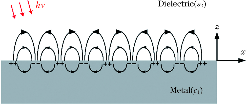
    Fig. 1. Schematic of plasmonic effect at metal-dielectric interface
    Energy distribution in crossed Au nanowires structure under polarized laser excitation[40-41](up: experimental results; down: simulation results. Wavelength: 532 nm)
    Fig. 2. Energy distribution in crossed Au nanowires structure under polarized laser excitation[40-41](up: experimental results; down: simulation results. Wavelength: 532 nm)
    Scaning electrons microscopy images of Ag nanowires after femtosecond laser irradiation[45].(a) Characterization of Ag nanowires ends after laser irradiation at different polarization directions; (b) characterization of Ag nanowires ends after laser irradiation for different times
    Fig. 3. Scaning electrons microscopy images of Ag nanowires after femtosecond laser irradiation[45].(a) Characterization of Ag nanowires ends after laser irradiation at different polarization directions; (b) characterization of Ag nanowires ends after laser irradiation for different times
    Different Ag nanowires structures after femtosecond laser nanojoining[45]. (a) “x”-shaped nanowire; (b) “y”-shaped nanowire; (c) nanowires network
    Fig. 4. Different Ag nanowires structures after femtosecond laser nanojoining[45]. (a) “x”-shaped nanowire; (b) “y”-shaped nanowire; (c) nanowires network
    Transmission electron microscopy images of branched Ag nanowire junction after femtosecond laser nanojoining[45]. (a) Cross sectional TEM image of joined Ag nanowire joint; (b) high resolution TEM image of the interface structure of Ag nanowire joint
    Fig. 5. Transmission electron microscopy images of branched Ag nanowire junction after femtosecond laser nanojoining[45]. (a) Cross sectional TEM image of joined Ag nanowire joint; (b) high resolution TEM image of the interface structure of Ag nanowire joint
    Electric field distribution around Ag-TiO2 nanowires structure under polarized laser irradiation[52]. (a) Simulated electric field intensity distribution around crossed Ag and TiO2 nanowires structure under polarized laser excitation with wavelength of 800 nm; (b) dependence of normalized electric field intensity at the junctions of different crossed nanowires structures with different angles on the incident laser polarization directions
    Fig. 6. Electric field distribution around Ag-TiO2 nanowires structure under polarized laser irradiation[52]. (a) Simulated electric field intensity distribution around crossed Ag and TiO2 nanowires structure under polarized laser excitation with wavelength of 800 nm; (b) dependence of normalized electric field intensity at the junctions of different crossed nanowires structures with different angles on the incident laser polarization directions
    Femtosecond laser nanojoining of heterogeneous metal-oxide nanowire structures[52]. (a) Femtosecond laser nanojoined Ag and TiO2 nanowires structure; (b) morphology of Ag and TiO2 nanowires junction after shear test; (c) EDX elemental mapping of femtosecond laser nanojoined Ag and TiO2 nanowires structure; (d) high resolution transmission electron microscopy image at the Ag-TiO2 nanowires interface
    Fig. 7. Femtosecond laser nanojoining of heterogeneous metal-oxide nanowire structures[52]. (a) Femtosecond laser nanojoined Ag and TiO2 nanowires structure; (b) morphology of Ag and TiO2 nanowires junction after shear test; (c) EDX elemental mapping of femtosecond laser nanojoined Ag and TiO2 nanowires structure; (d) high resolution transmission electron microscopy image at the Ag-TiO2 nanowires interface
    Femtosecond laser nanojoining of cross-dimensional heterogeneous nanowire structures[55]. (a) Normalized electric field intensity distribution around TiO2 nanowire-Au electrodes under polarized laser excitation with wavelength of 800 nm; (b)(c) SEM images of femtosecond laser nanojoined TiO2 nanowire-Au electrodes structures; (d) AFM image of TiO2 nanowire-Au electrodes structures shown in Fig.8(c) after strength test by AFM probe
    Fig. 8. Femtosecond laser nanojoining of cross-dimensional heterogeneous nanowire structures[55]. (a) Normalized electric field intensity distribution around TiO2 nanowire-Au electrodes under polarized laser excitation with wavelength of 800 nm; (b)(c) SEM images of femtosecond laser nanojoined TiO2 nanowire-Au electrodes structures; (d) AFM image of TiO2 nanowire-Au electrodes structures shown in Fig.8(c) after strength test by AFM probe
    Femtosecond laser nanojoining of transparent Ag nanowires electrodes[57]. (a) Transmittance of Ag nanowires electrodes fabricated under different femtosecond laser fluences; (b) transmittance and resistance of Ag nanowires electrodes fabricated by different nanojoining process(laser wavelength: 800 nm)
    Fig. 9. Femtosecond laser nanojoining of transparent Ag nanowires electrodes[57]. (a) Transmittance of Ag nanowires electrodes fabricated under different femtosecond laser fluences; (b) transmittance and resistance of Ag nanowires electrodes fabricated by different nanojoining process(laser wavelength: 800 nm)
    Fabrication of transparent Ag nanowires electrodes by femtosecond laser and nanosecond laser nanojoining[57]. (a) Transmittance and surface roughness of PET substrates after femtosecond laser irradiation at different fluences; (b) transmittance and surface roughness of PET substrates after nanosecond laser irradiation at different fluences; (c) morphology of Ag nanowires structures damaged by femtosecond laser; (d) morphology of Ag nanowires structures damaged by nanosecond laser irradiation
    Fig. 10. Fabrication of transparent Ag nanowires electrodes by femtosecond laser and nanosecond laser nanojoining[57]. (a) Transmittance and surface roughness of PET substrates after femtosecond laser irradiation at different fluences; (b) transmittance and surface roughness of PET substrates after nanosecond laser irradiation at different fluences; (c) morphology of Ag nanowires structures damaged by femtosecond laser; (d) morphology of Ag nanowires structures damaged by nanosecond laser irradiation
    Femtosecond laser nanojoined TiO2 nanowire and Au electrodes structures(laser wavelength: 800 nm)[55]. (a)(c) Morphology and electrical response of nanojoined nanowire structure at low laser fluence; (b)(d) morphology and electrical response of nanojoined nanowire structure at high laser fluence
    Fig. 11. Femtosecond laser nanojoined TiO2 nanowire and Au electrodes structures(laser wavelength: 800 nm)[55]. (a)(c) Morphology and electrical response of nanojoined nanowire structure at low laser fluence; (b)(d) morphology and electrical response of nanojoined nanowire structure at high laser fluence
    Multilevel memory characteristic of femtosecond laser joined TiO2 nanowire-Au electrodes structure[55]
    Fig. 12. Multilevel memory characteristic of femtosecond laser joined TiO2 nanowire-Au electrodes structure[55]
    Fabrication of nanowire-based electronic unit with multiple dielectric layers by femtosecond laser nanojoining[59]. (a) Electrical response of core-shell SiC-SiO2 nanowire-Au electrodes structures joined by femtosecond laser; (b) SEM image of nanowire-electrodes structure after electrical break-down; (c)(d) magnified images of localized structures of nanowire shown in Fig.13(b)
    Fig. 13. Fabrication of nanowire-based electronic unit with multiple dielectric layers by femtosecond laser nanojoining[59]. (a) Electrical response of core-shell SiC-SiO2 nanowire-Au electrodes structures joined by femtosecond laser; (b) SEM image of nanowire-electrodes structure after electrical break-down; (c)(d) magnified images of localized structures of nanowire shown in Fig.13(b)
    Fabrication of single nanowire sensor by femtosecond laser nanojoining[60]. (a) Resistance of single nanowire sensor measured at different glucose concentrations; (b) current response of single nanowire sensor with increasing glucose concentration
    Fig. 14. Fabrication of single nanowire sensor by femtosecond laser nanojoining[60]. (a) Resistance of single nanowire sensor measured at different glucose concentrations; (b) current response of single nanowire sensor with increasing glucose concentration
    Optical transportation of branched Ag nanowires structure(laser wavelength: 800 nm)[18,45]. (a) Simulation results of branched Ag nanowires structures before nanojoining process; (b) simulation results of branched Ag nanowires structures after nanojoining process; (c) dependence of optical transportation at nanowire ends with incident laser polarization directions; (d) dark field images illustrating the optical transportation of branched Ag nanowires structure before and after nanojoining process
    Fig. 15. Optical transportation of branched Ag nanowires structure(laser wavelength: 800 nm)[18,45]. (a) Simulation results of branched Ag nanowires structures before nanojoining process; (b) simulation results of branched Ag nanowires structures after nanojoining process; (c) dependence of optical transportation at nanowire ends with incident laser polarization directions; (d) dark field images illustrating the optical transportation of branched Ag nanowires structure before and after nanojoining process
    Luchan Lin, Songling Xing, Jinpeng Huo, Yu Xiao, Peng Peng, Daozhi Shen, Lei Liu, Guisheng Zou. Research Progress of Ultrafast Laser-Induced Nanowires Joining Technology[J]. Chinese Journal of Lasers, 2021, 48(8): 0802001
    Download Citation