
Yun Cui, Yuanan Zhao, Ge Zhang, Meiping Zhu, Chen Song, Chunxian Tao, Tan Shu, Jianda Shao. Influence of annealing temperature on the performance of TiO2/SiO2 nanolaminated films[J]. Chinese Optics Letters, 2021, 19(12): 121406
- Chinese Optics Letters
- Vol. 19, Issue 12, 121406 (2021)
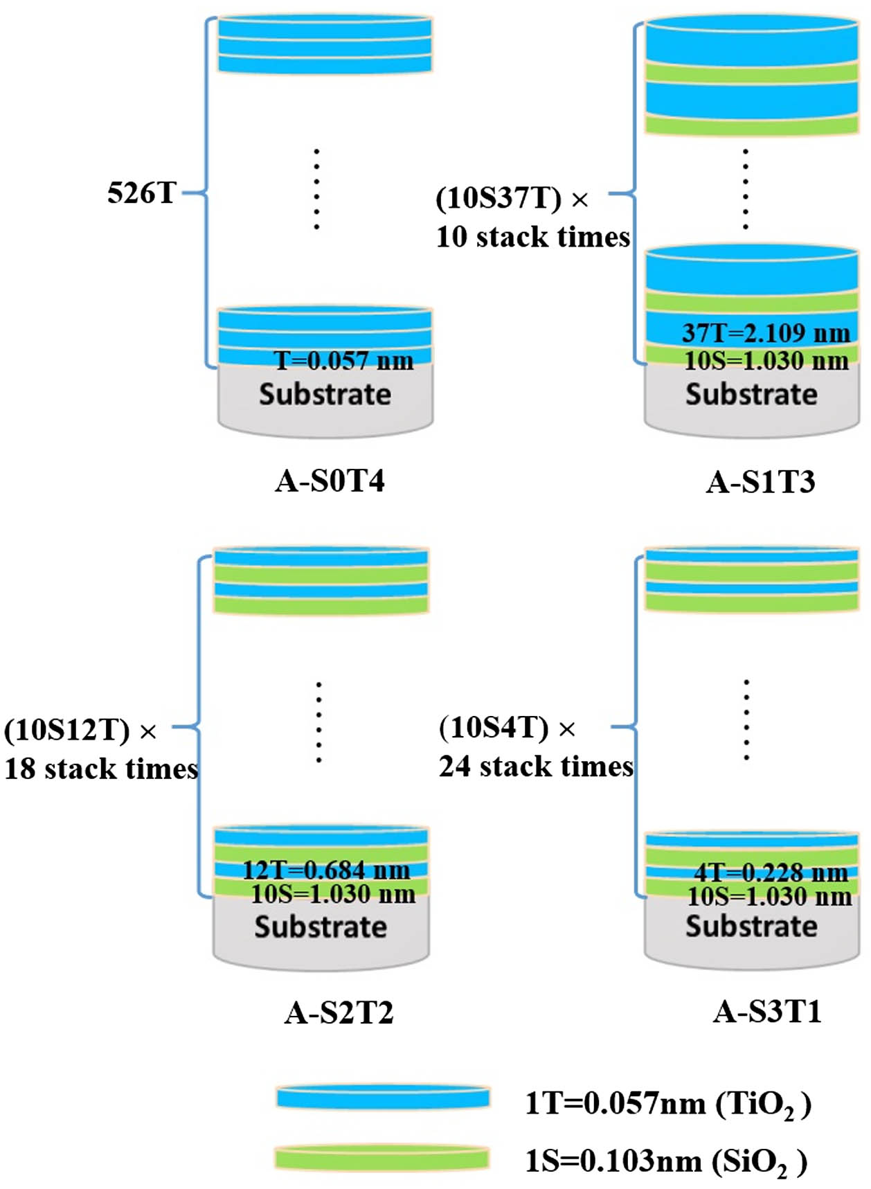
Fig. 1. Schematic diagrams of the structures of the nanolaminated films.
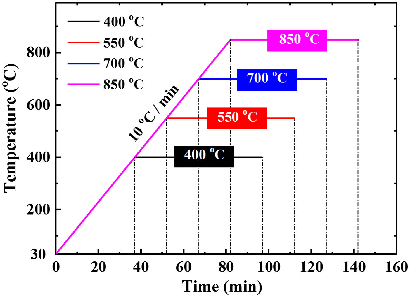
Fig. 2. Annealing programs of the samples at 400°C, 550°C, 700°C, and 850°C.
Fig. 3. Diffraction spectra of sample A-S0T4 before and after annealing; the inset shows the change in the diffraction angle.
Fig. 4. Surface morphologies of sample A-S0T4 before and after annealing: (a) before annealing, (b) after annealing at 400°C, (c) after annealing at 700°C, and (d) after annealing at 850°C.
Fig. 5. Diffraction spectra of the samples before and after annealing: (a) A-S1T3, (b) A-S2T2, and (c) A-S3T1.
Fig. 6. Surface morphologies of the samples before and after annealing: (a) before annealing of A-S1T3, (b) after annealing of A-S1T3 at 850°C, (c) before annealing of A-S2T2, (d) after annealing of A-S2T2 at 850°C, (e) before annealing of A-S3T1, and (f) after annealing of A-S3T1 at 850°C.
Fig. 7. XRR curves of sample A-S0T4 before and after annealing.
Fig. 8. Changes in the thickness and density of the four types of films with the annealing temperature.
Fig. 9. Changes in the elemental composition of the four types of films before and after annealing at 850°C.
Fig. 10. BE spectra for the four elements in different samples. (a) Ti 2p XPS core-line spectra: the BEs of Ti increased with decrease in the Ti content in the film before annealing. (b) Si 2p XPS core-line spectra: the BEs of Si increased with decrease in the Ti content in the film before annealing. (c) O 1s XPS core-line spectra: the BEs of O increased with decrease in the Ti content in the film before annealing. (d) Al 2p XPS core-line spectra: the BEs of Al increased with decrease in the Ti content in the film after annealing at 850°C.
Fig. 11. O 1s XPS core-line spectrum and the peak-fitting situation in sample A-S2T2 (a) before baking and (b) after annealing at 850°C.
|
Table 1. One Cycle of the SiO 2 TiO 2
|
Table 2. Design Structures of the Nanolaminated Films
|
Table 3. Atomic Percentage and BE of Each Constituent Element of Sample A-S2T2 before and after Annealing at 850°C

Set citation alerts for the article
Please enter your email address
© Copyright 2018-2021 | Chinese Laser Press. All Rights Reserved 沪ICP备15018463号-20