
Yun Cui, Yuanan Zhao, Ge Zhang, Meiping Zhu, Chen Song, Chunxian Tao, Tan Shu, Jianda Shao, "Influence of annealing temperature on the performance of TiO2/SiO2 nanolaminated films," Chin. Opt. Lett. 19, 121406 (2021)
- Chinese Optics Letters
- Vol. 19, Issue 12, 121406 (2021)
Abstract
1. Introduction
Titania (
In summary,
Sign up for Chinese Optics Letters TOC. Get the latest issue of Chinese Optics Letters delivered right to you!Sign up now
Herein, ALD was used to prepare the
2. Experiments
2.1. Sample preparation
One cycle of
![]()
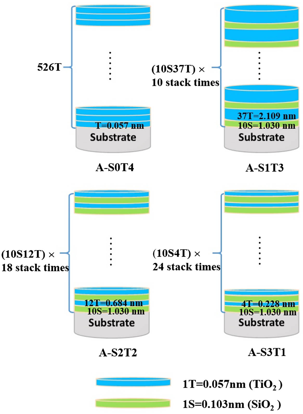
Figure 1.Schematic diagrams of the structures of the nanolaminated films.
| Deposited Film | Precursor | Purity (N) | Precursor Temperature | Reaction Temperature (°C) | Thickness of One Circle (nm) |
|---|---|---|---|---|---|
| 3DMAS ( | Room | 150 | 0.103 (S) | ||
| TDMAT ( | 90°C | 150 | 0.057 (T) |
Table 1. One Cycle of the
| Sample | Total Thickness (nm) | Nano-Laminated Structure | Substrate |
|---|---|---|---|
| A-S0T4 | 30 | Sub/526T × 1 stack time | |
| A-S1T3 | 30 | Sub/(10S37T) × 10 stack times | |
| A-S2T2 | 30 | Sub/(10S12T) × 18 stack times | |
| A-S3T1 | 30 | Sub/(10S4T) × 24 stack times |
Table 2. Design Structures of the Nanolaminated Films
2.2. Experimental conditions and sample characterization
The prepared samples were annealed at different temperatures. The samples were transferred to a quartz glass tube furnace for annealing treatment. The temperature of the furnace was raised from room temperature to 400°C, 550°C, 700°C, and 850°C sequentially; the heating rate was 10°C/min, and the set temperature was maintained for 1 h, as shown in Fig. 2. Finally, the sample was naturally cooled to room temperature.
![]()
Figure 2.Annealing programs of the samples at 400°C, 550°C, 700°C, and 850°C.
Surface morphologies were analyzed via field emission scanning electron microscopy (FESEM; Auriga, Zeiss). The resolution was 1 nm for the electron beam at 15 kV. The acceleration voltage varied continuously from 0.1 to 30 kV at 10 V intervals. The magnification range was 12–
Phase identification and film thickness analyses were conducted via X-ray diffraction (XRD; Empyream, PANalytical) in the continuous scanning mode, using Cu Kα1 radiation (
Component analysis was conducted through X-ray photoelectron spectroscopy (XPS; KAlpha, Thermo Scientific) using a monochromatic Al Kα source, with a characteristic emission line of 1486.6 eV. The depth profile was cut using
3. Results
3.1. Crystal phase and surface morphologies
The crystalline phase and surface morphologies of the four samples before and after annealing were analyzed. As shown in Fig. 3, sample A-S0T4 did not crystallize after annealing at 400°C, and the anatase phase (reference ICDD code: 00-002-0406) appeared after annealing at 550°C, indicating that its phase transition temperature was between 400°C and 550°C; the anatase phase of the film remained until after annealing at 850°C. The inset of Fig. 3 shows that as the annealing temperature increased, the diffraction angle increased slightly, indicating that the interplanar spacing decreased as the annealing temperature increased. Figure 4 presents the surface morphologies of sample A-S0T4 before and after baking at different temperatures. No change in the surface morphologies was observed before and after annealing at 400°C, as shown in Figs. 4(a) and 4(b), and large grains appeared on the surface of the film after annealing at 550°C, as shown in Fig. 4(c). With an increase in the annealing temperature, the sizes of the particles of
![]()
Figure 3.Diffraction spectra of sample A-S0T4 before and after annealing; the inset shows the change in the diffraction angle.
![]()
Figure 4.Surface morphologies of sample A-S0T4 before and after annealing: (a) before annealing, (b) after annealing at 400°C, (c) after annealing at 700°C, and (d) after annealing at 850°C.
The films on A-S1T3 and A-S2T2 were amorphous before annealing, as shown in Figs. 5(a) and 5(b). The crystallization temperature increased with the increase in the
![]()
Figure 5.Diffraction spectra of the samples before and after annealing: (a) A-S1T3, (b) A-S2T2, and (c) A-S3T1.
![]()
Figure 6.Surface morphologies of the samples before and after annealing: (a) before annealing of A-S1T3, (b) after annealing of A-S1T3 at 850°C, (c) before annealing of A-S2T2, (d) after annealing of A-S2T2 at 850°C, (e) before annealing of A-S3T1, and (f) after annealing of A-S3T1 at 850°C.
3.2. Thickness and density
The thickness and density changes of four types of films were analyzed by measuring the XRR curves. As shown in Fig. 7, according to the critical angle of the curve, distance of oscillations, and shape of the curve, the density and thickness of the films were fitted and analyzed. Figure 8 shows the fitting results; the thickness was normalized. Results showed that as the annealing temperature increased, the film thickness decreased, and the density increased.
![]()
Figure 7.XRR curves of sample A-S0T4 before and after annealing.
![]()
Figure 8.Changes in the thickness and density of the four types of films with the annealing temperature.
3.3. Changes in the ingredient content and BE
The elemental composition of the four samples before and after annealing at 850°C was analyzed via XPS, and Fig. 9 shows the results. The content of Si gradually increased from sample A-S0T4 to sample A-S3T1, which was consistent with the design trend; however, the Si content was significantly less than the design result, which was attributed to the
![]()
Figure 9.Changes in the elemental composition of the four types of films before and after annealing at 850°C.
The changes in the BEs of Si, Ti, and O before annealing and the changes in the BEs of Al after annealing at 850°C in the four types of samples were analyzed, and Fig. 10 shows the results. The BEs of Ti, Si, and Al in films were between those of the pure elements and those of the pure oxides; these indicated that the nanolaminated films exhibited a complex bonding structure. The BEs of Ti, Si, and Al increased with the decrease of Ti content in the films, as shown in Figs. 10(a), 10(b), and 10(d), and the BEs shifts were caused by the substitution of Si or Al for Ti atoms, which was much less electronegative[
![]()
Figure 10.BE spectra for the four elements in different samples. (a) Ti 2p XPS core-line spectra: the BEs of Ti increased with decrease in the Ti content in the film before annealing. (b) Si 2p XPS core-line spectra: the BEs of Si increased with decrease in the Ti content in the film before annealing. (c) O 1s XPS core-line spectra: the BEs of O increased with decrease in the Ti content in the film before annealing. (d) Al 2p XPS core-line spectra: the BEs of Al increased with decrease in the Ti content in the film after annealing at 850°C.
The BE spectra of O showed a multipeak state, indicating that O comprised a variety of chemical bonds, as shown in Fig. 10(c).
As shown in Figs. 11(a) and 11(b), the O 1s XPS core-line spectra of sample A-S2T2 were subjected to peak splitting before and after annealing. Table 3 shows the atomic percentage and BEs. Al ions diffused into the film, and the O 1s XPS core-line spectrum also changed accordingly after annealing at 850°C. This indicated that a chemical bond was formed between the Al ions and O ions. The structure of the mixed oxide film was extremely complicated[
| State | Type | Ti 2p | Si 2p | Al 2p | O 1s A (Ti–O) | O 1s B (Si–O) | O 1s C (Al–O) |
|---|---|---|---|---|---|---|---|
| Before baking | Atomic percentage (%) | 26.0 | 9.0 | – | 46.2 | 18.8 | – |
| Binding energy (eV) | 457.8 | 101.1 | – | 529.5 | 530.6 | – | |
| After baking | Atomic percentage (%) | 18.9 | 11.1 | 5.7 | 29.8 | 22.7 | 11.8 |
| Binding energy (eV) | 458.0 | 102.1 | 73.1 | 529.6 | 531.6 | 530.7 |
Table 3. Atomic Percentage and BE of Each Constituent Element of Sample A-S2T2 before and after Annealing at 850°C
![]()
Figure 11.O 1s XPS core-line spectrum and the peak-fitting situation in sample A-S2T2 (a) before baking and (b) after annealing at 850°C.
4. Discussion
Herein, four types of
Results showed that the
The crystallization temperature of the films was proportional to the
The Al ions in the substrates diffused into the four types of nanolaminated films and bonded with O after 850°C annealing. In the subsequent tests, the elemental percentages of the four types of thin films on the
References
[1] A. I. Abdulagatov, Y. Yan, J. R. Cooper, Y. Zhang. Al2O3 and TiO2 atomic layer deposition on copper for water corrosion resistance. ACS Appl. Mater. Interfaces, 3, 4593(2011).
[2] H. Xiong, Y. Tang, L. Hu, H. Li. An ORMOSIL porous double-layer broadband antireflective coating. Chin. Opt. Lett., 17, 033101(2019).
[3] C. Shan, Y. A. Zhao, Y. Q. Gao. Laser-induced defects in optical multilayer coatings by the spatial resolved method. Chin. Opt. Lett., 17, 031403(2019).
[4] L. M. Pastrana-Martínez, S. Morales-Torres, S. A. Carabineiro, J. G. Buijnsters, J. L. Figueiredo, A. M. Silva, J. L. Faria. Photocatalytic activity of functionalized nanodiamond-TiO2 composites towards water pollutants degradation under UV/Vis irradiation. Appl. Surf. Sci., 458, 839(2018).
[5] A. R. Khataee, M. Zarei, R. Ordikhani-Seyedlar. Heterogeneous photocatalysis of a dye solution using supported TiO2 nanoparticles combined with homogeneous photoelectrochemical process: molecular degradation products. J. Mol. Catal. A, 338, 84(2011).
[6] Z.-H. Liu, G.-L. Hou, X.-J. Su. Effects of heat treatment temperature on photocatalytic activity of TiO2/SiO2 composite aerogels. J. Inorg. Mater., 27, 1079(2012).
[7] J. O. Haolat, A. George, M. Issa Suleiman, M. Berthod, K. Wang. UV-TiO2 treatment of the cooling water of an oil refinery. J. Water Process Eng., 26, 176(2018).
[8] A. Abbasi, D. Ghanbari, M. Salavati-Niasari, M. Hamadanian. Photo-degradation of methylene blue: photocatalyst and magnetic investigation of Fe2O3–TiO2 nanoparticles and nanocomposites. J. Mater. Sci.: Mater. Electron., 27, 4800(2016).
[9] A. L. Linsebigler, G. Lu, J. T. Yates. Photocatalysis on TiO2 surfaces: principles, mechanisms, and selected results. Chem. Rev., 95, 735(1995).
[10] M. J. Guardalben, M. Barczys, B. E. Kruschwitz, M. Spilatro, L. J. Waxer, E. M. Hill. Laser-system model for enhanced operational performance and flexibility on OMEGA EP. High Power Laser Sci. Eng., 8, e8(2020).
[11] F. Zhang, S. Jin, Y. Mao. Surface characterization of titanium oxide films synthesized by ion beam enhanced deposition. Thin Solid Films, 310, 29(1997).
[12] L. Sirghi, T. Aoki, Y. Hatanaka. Hydrophilicity of TiO2 thin films obtained by radio frequency magnetron sputtering deposition. Thin Solid Films, 422, 55(2002).
[13] D. Benz, H. V. Bui, H. T. Hintzen, M. T. Kreutzer, J. Ruud van Ommen. Synthesis of a rationally designed multi-component photocatalyst Pt:SiO2:TiO2(P25) with improved activity for dye degradation by atomic layer deposition. Nanomaterials, 10, 1496(2020).
[14] S. Yaparatne, C. P. Tripp, A. Amirbahman. Photodegradation of taste and odor compounds in water in the presence of immobilized TiO2-SiO2 photocatalysts. J. Hazard. Mater., 346, 208(2018).
[15] E. Rahmani, M. Rahmani, H. R. Silab. TiO2:SiO2 thin film coated annular photoreactor for degradation of oily contamination from waste water. J. Water Process Eng., 37, 101374(2020).
[16] L. H. Gan, Y. D. Wang, Z. X. Hao. Preparation of TiO2/SiO2 aerogels by non-supercritical drying method and their photocatalytic activity for degradation of pyridine. Chin. J. Chem. Eng., 13, 758(2005).
[17] Z.-H. Liu, X.-J. Su, G.-L. Hou. Effects of silicon content on microstructure and photocatalytic activity of TiO2/SiO2 composite aerogels. J. Inorg. Mater., 25, 911(2010).
[18] S. Mortazavi-Derazkola, M. Salavati-Niasari, O. Amiri, A. Abbasi. Fabrication and characterization of Fe3O4@SiO2@TiO2@Ho nanostructures as a novel and highly efficient photocatalyst for degradation of organic pollution. J. Energy Chem., 26, 17(2017).
[19] A. Brunet-Bruneau, S. Fisson, B. Gallas, G. Vuye, J. Rivory. Optical properties of mixed TiO2-SiO2 films, from infrared to ultraviolet. Proc. SPIE, 3738, 188(1999).
[20] V. G. Dyskin, I. A. Tursunbaev. Antireflection coatings for solar photoelectric elements based on SiO2 and TiO2 mixed oxides. Appl. Solar Energy, 47, 137(2011).
[21] E. Riyanto, E. Martides, E. Junianto, B. Prawara. The growth mechanisms of atomic layer deposition: an overview. Eksergi, 17, 56(2020).
[22] M. W. Gaultois, A. P. Grosvenor. XANES and XPS investigations of the local structure and final-state effects in amorphous metal silicates: (ZrO2)x(TiO2)y(SiO2)1-x-y. Phys. Chem. Chem. Phys., 14, 205(2012).
[23] B. M. Reddy, B. Chowdhury, P. G. Smirniotis. An XPS study of the dispersion of MoO3 on TiO2-ZrO2, TiO2-SiO2, TiO2-Al2O3, SiO2-ZrO2, and SiO2-TiO2-ZrO2 mixed oxides. Appl. Catal. A, 211, 19(2001).


Set citation alerts for the article
Please enter your email address

© Copyright 2018-2021 | Chinese Laser Press. All Rights Reserved 沪ICP备15018463号-20