
Meng Zhang, Ruo-He Yao, Yu-Rong Liu, Kui-Wei Geng. Shot noise model of the short channel metal-oxide-semiconductor field-effect transistor [J]. Acta Physica Sinica, 2020, 69(17): 177102-1
- Acta Physica Sinica
- Vol. 69, Issue 17, 177102-1 (2020)
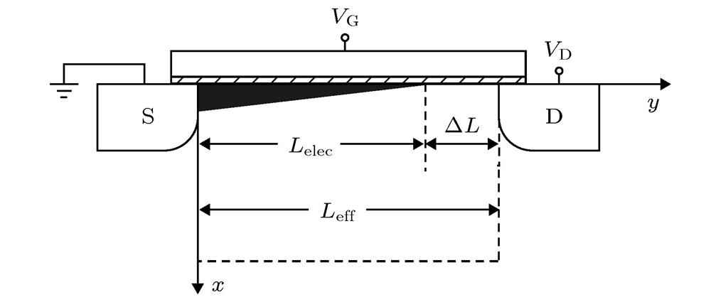
Fig. 1. Structure diagram of the NMOSFET device.
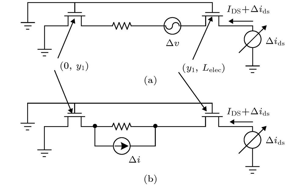
Fig. 2. Schematic diagram of the transistor with a fictitious dc source in the channel.
Fig. 3. Full-shot noise and thermal noise vs . gate-source bias voltage (L eff = 40 nm).
Fig. 4. Fano factor of shot noise vs . gate-source bias voltage (L eff = 40 nm).
Fig. 5. Full-shot noise and thermal noise vs . gate-source bias voltage (L eff = 20 nm).
Fig. 6. Fano factor of shot noise vs . gate-source bias voltage (L eff = 20 nm).
Fig. 7. Full-shot noise and thermal noise vs . gate-source bias voltage (L eff = 10 nm).
Fig. 8. Fano factor of shot noise vs. gate-source bias voltage (L eff = 10 nm).

Set citation alerts for the article
Please enter your email address
© Copyright 2018-2021 | Chinese Laser Press. All Rights Reserved 沪ICP备15018463号-20