• Advanced Photonics
  • Vol. 5, Issue 4, 046003 (2023)
Liu Yang1、†, Zhanke Zhou1, Hao Wu1, Hongliang Dang1, Yuxin Yang1, Jiaxin Gao1, Xin Guo1、2, Pan Wang1、2, and Limin Tong1、2、3、*
Author Affiliations
  • 1Zhejiang University, College of Optical Science and Engineering, New Cornerstone Science Laboratory, Interdisciplinary Center for Quantum Information, Hangzhou, China
  • 2Jiaxing Institute of Zhejiang University, Intelligent Optics and Photonics Research Center, Jiaxing, China
  • 3Shanxi University, Collaborative Innovation Center of Extreme Optics, Taiyuan, China
  • show less
    DOI: 10.1117/1.AP.5.4.046003 Cite this Article Set citation alerts
    Liu Yang, Zhanke Zhou, Hao Wu, Hongliang Dang, Yuxin Yang, Jiaxin Gao, Xin Guo, Pan Wang, Limin Tong. Generating a sub-nanometer-confined optical field in a nanoslit waveguiding mode[J]. Advanced Photonics, 2023, 5(4): 046003 Copy Citation Text show less
    Schematic illustration of the CNP waveguiding scheme. (a) Freestanding CNP waveguide, coupled by a fiber taper drawn from a standard glass fiber. (b) On-chip CNP waveguide, coupled by a tapered planar waveguide.
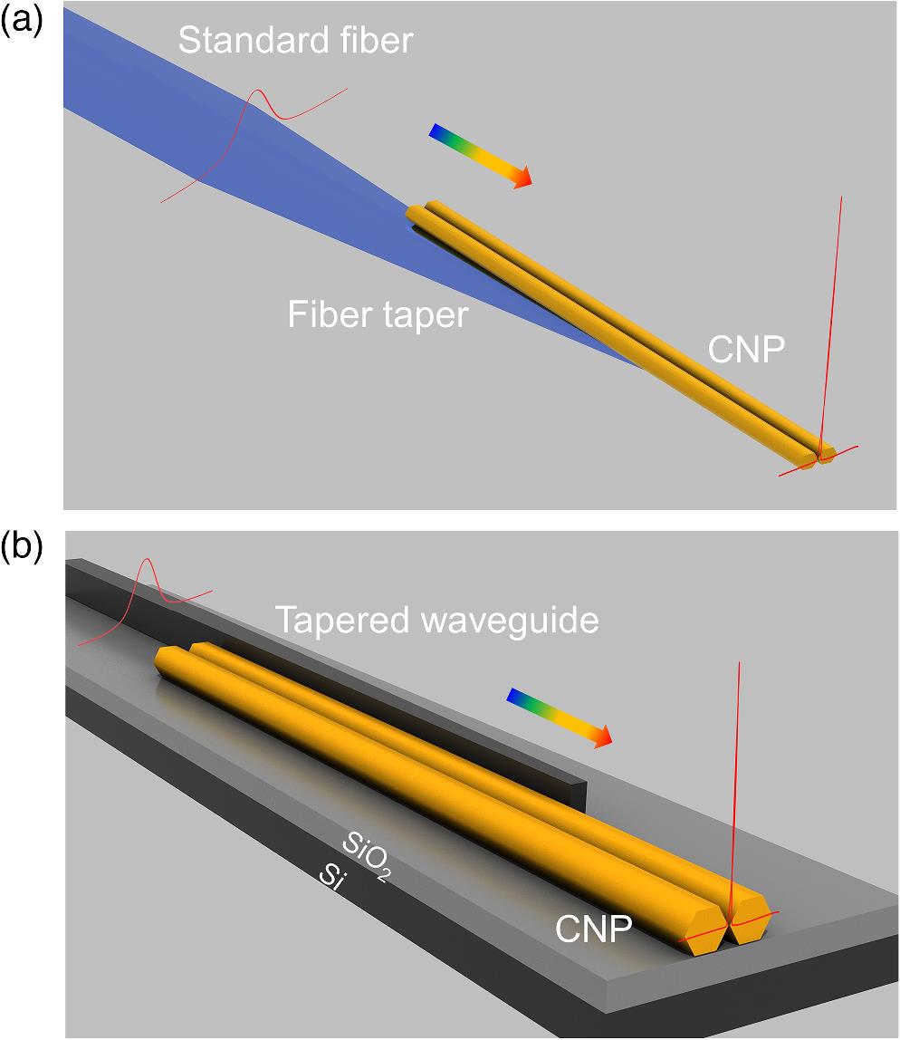
    Fig. 1. Schematic illustration of the CNP waveguiding scheme. (a) Freestanding CNP waveguide, coupled by a fiber taper drawn from a standard glass fiber. (b) On-chip CNP waveguide, coupled by a tapered planar waveguide.
    Four lowest eigenmodes of a CNP waveguide. Normalized electric field distribution (left panel) and surface polarized bound charge density distribution (right panel) of (a) TE0-like, (b) TM0-like, (c) TE1-like, and (d) TM1-like modes in a CdS CNP with a nanowire diameter of 180 nm at 550-nm wavelength. The scale bar in (a) applies to (b)–(d). (e)–(h) Diameter-dependent neff of the four lowest modes of (e) a freestanding CNP at 550-nm wavelength, (f) a freestanding CNP at 750-nm wavelength, (g) an on-chip CNP at 550-nm wavelength, and (h) an on-chip CNP at 650-nm wavelength. The blue-shaded areas represent the selected diameter areas in this work. The dashed black lines indicate the refractive index of the substrate.
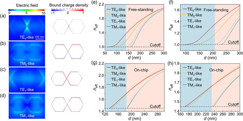
    Fig. 2. Four lowest eigenmodes of a CNP waveguide. Normalized electric field distribution (left panel) and surface polarized bound charge density distribution (right panel) of (a) TE0-like, (b) TM0-like, (c) TE1-like, and (d) TM1-like modes in a CdS CNP with a nanowire diameter of 180 nm at 550-nm wavelength. The scale bar in (a) applies to (b)–(d). (e)–(h) Diameter-dependent neff of the four lowest modes of (e) a freestanding CNP at 550-nm wavelength, (f) a freestanding CNP at 750-nm wavelength, (g) an on-chip CNP at 550-nm wavelength, and (h) an on-chip CNP at 650-nm wavelength. The blue-shaded areas represent the selected diameter areas in this work. The dashed black lines indicate the refractive index of the substrate.
    Mode evolution in a freestanding CdS CNP waveguide. (a) Schematic diagram of the coupling structure. A horizontal coordinate indicates the waveguide length originated from the left end of the CNP. The blue dashed line indicates the obscured profile of the fiber taper beneath the CNP. (b)–(e) Field intensity distribution in y−z planes (cross-sectional planes) at corresponding x positions marked by yellow arrows. The simulation is carried out with a nanowire diameter of 140 nm and a fiber-taper angle of 3 deg at 650-nm wavelength. The insets in (d) and (e) are close-up views of the field intensity around the CNP. The scale bar in (b) applies to (c)–(e). (f) neff of the HE11 mode of the fiber taper and the nanoslit TE0-like mode of the CNP within the spectral range of 550 to 750 nm. The blue and pink areas indicate the nanoslit mode and the HE11 mode, respectively. The intersecting red area is the neff-matching area of the two modes within the spectral range of 550 to 750 nm, and the solid yellow line represents the matched neff of the two modes at the same wavelength with respect to the fiber taper diameter (see Sec. S4 in the Supplemental Material). (g) Broadband coupling efficiency and mode purity of the TE0-like nanoslit mode.
    Fig. 3. Mode evolution in a freestanding CdS CNP waveguide. (a) Schematic diagram of the coupling structure. A horizontal coordinate indicates the waveguide length originated from the left end of the CNP. The blue dashed line indicates the obscured profile of the fiber taper beneath the CNP. (b)–(e) Field intensity distribution in yz planes (cross-sectional planes) at corresponding x positions marked by yellow arrows. The simulation is carried out with a nanowire diameter of 140 nm and a fiber-taper angle of 3 deg at 650-nm wavelength. The insets in (d) and (e) are close-up views of the field intensity around the CNP. The scale bar in (b) applies to (c)–(e). (f) neff of the HE11 mode of the fiber taper and the nanoslit TE0-like mode of the CNP within the spectral range of 550 to 750 nm. The blue and pink areas indicate the nanoslit mode and the HE11 mode, respectively. The intersecting red area is the neff-matching area of the two modes within the spectral range of 550 to 750 nm, and the solid yellow line represents the matched neff of the two modes at the same wavelength with respect to the fiber taper diameter (see Sec. S4 in the Supplemental Material). (g) Broadband coupling efficiency and mode purity of the TE0-like nanoslit mode.
    Sub-nm-confined optical fields in the nanoslit mode at visible spectrum. (a) Normalized cross-sectional field intensity distribution of the TE0-like nanoslit mode of a CdS CNP with d=140 nm, w=1 nm, r=5 nm, and λ=550 nm. The coordinate origin is located at the center of the slit. (b) FWHM of the field intensity of the TE0-like mode along the x axis (blue line) and y axis (orange line) with λ=550 nm. (c) λ-dependent FWHM of the field intensity along the x axis (blue line) and y axis (orange line). (d) Power density (Poynting vector in the z direction, Pz) distribution around the slit cross section. The closed white line indicates the contour of Pz(0, 0)/2, marking the profile of the central hot spot. (e) Overall Pz distribution around the CNP cross section in a log scale. The closed white line indicates the boundary of the effective mode area. The units of all coordinates of (d) and (e) are nanometers. (f) 3-D plot of the normalized cross-sectional field intensity distribution of the TE0-like nanoslit mode. (g) Field intensity distribution along the x-axis direction. For better clarity, a 100× profile is also plotted as dotted lines. (h) λ-dependent peak-to-background ratio RP1/B (blue line) and RP2/B (orange line) of the TE0-like nanoslit mode, respectively.
    Fig. 4. Sub-nm-confined optical fields in the nanoslit mode at visible spectrum. (a) Normalized cross-sectional field intensity distribution of the TE0-like nanoslit mode of a CdS CNP with d=140  nm, w=1  nm, r=5  nm, and λ=550  nm. The coordinate origin is located at the center of the slit. (b) FWHM of the field intensity of the TE0-like mode along the x axis (blue line) and y axis (orange line) with λ=550  nm. (c) λ-dependent FWHM of the field intensity along the x axis (blue line) and y axis (orange line). (d) Power density (Poynting vector in the z direction, Pz) distribution around the slit cross section. The closed white line indicates the contour of Pz(0, 0)/2, marking the profile of the central hot spot. (e) Overall Pz distribution around the CNP cross section in a log scale. The closed white line indicates the boundary of the effective mode area. The units of all coordinates of (d) and (e) are nanometers. (f) 3-D plot of the normalized cross-sectional field intensity distribution of the TE0-like nanoslit mode. (g) Field intensity distribution along the x-axis direction. For better clarity, a 100× profile is also plotted as dotted lines. (h) λ-dependent peak-to-background ratio RP1/B (blue line) and RP2/B (orange line) of the TE0-like nanoslit mode, respectively.
    Sub-nm-confined optical fields in the nanoslit mode at MIR spectrum. (a) Normalized cross-sectional field intensity distribution of the TE0-like nanoslit mode of a CdS CNP with d=1 μm, w=1 nm, r=5 nm, and λ=3.7 μm. (b) λ-dependent FWHM of the field intensity along the x axis (solid line) and y axis (dashed line) of a CdS CNP and a CdTe CNP with the same geometries, respectively. (c) Pz distribution around the slit cross section. The closed white line indicates the contour of Pz(0, 0)/2, marking the profile of the central hot spot. (d) Overall Pz distribution around the CNP cross section in a log scale. The closed white line indicates the boundary of the effective mode area. The units of all coordinates of (c) and (d) are nanometers. (e) λ-dependent peak-to-background ratio RP1/B (solid line) and RP2/B (dashed line) of the TE0-like nanoslit mode of CdS and CdTe CNPs, respectively.
    Fig. 5. Sub-nm-confined optical fields in the nanoslit mode at MIR spectrum. (a) Normalized cross-sectional field intensity distribution of the TE0-like nanoslit mode of a CdS CNP with d=1  μm, w=1  nm, r=5  nm, and λ=3.7  μm. (b) λ-dependent FWHM of the field intensity along the x axis (solid line) and y axis (dashed line) of a CdS CNP and a CdTe CNP with the same geometries, respectively. (c) Pz distribution around the slit cross section. The closed white line indicates the contour of Pz(0, 0)/2, marking the profile of the central hot spot. (d) Overall Pz distribution around the CNP cross section in a log scale. The closed white line indicates the boundary of the effective mode area. The units of all coordinates of (c) and (d) are nanometers. (e) λ-dependent peak-to-background ratio RP1/B (solid line) and RP2/B (dashed line) of the TE0-like nanoslit mode of CdS and CdTe CNPs, respectively.
    λ-dependent Vg and D of the nanoslit mode in a CdS CNP at (a) visible spectrum with d=140 nm and (b) MIR spectrum with d=1 μm. In all calculations, w is assumed to be 1 nm and r is assumed to be 5 nm.
    Fig. 6. λ-dependent Vg and D of the nanoslit mode in a CdS CNP at (a) visible spectrum with d=140  nm and (b) MIR spectrum with d=1  μm. In all calculations, w is assumed to be 1 nm and r is assumed to be 5 nm.
    Liu Yang, Zhanke Zhou, Hao Wu, Hongliang Dang, Yuxin Yang, Jiaxin Gao, Xin Guo, Pan Wang, Limin Tong. Generating a sub-nanometer-confined optical field in a nanoslit waveguiding mode[J]. Advanced Photonics, 2023, 5(4): 046003
    Download Citation