State Key Laboratory of High Performance and Complex Manufacturing, College of Mechanical and Electrical Engineering, Central South University, Changsha 410083, China
In this study, we propose an effective method for the fabrication of annulus micro-/nanostructures by a femtosecond laser doughnut beam. Compared with the traditional Bessel annulus beam shaping system, this method greatly compresses the light propagation path. It is theoretically and experimentally demonstrated that the obtained axial section of the peak envelope in the processing area is two waists of the isosceles triangle. By moving the relative position of the sample, annulus microstructures with different diameters on copper sheet could be fabricated. In addition, laser induced periodic surface structures with controllable direction are fabricated by this optical system.
Due to the advantages of small size, light weight, and low cost, micro-optical components are the key devices for micro optoelectronic systems. For numerous micro-optical components such as optical antennas[1–3], sensors[4–7], color filters[8,9], and diffraction optical devices[10,11], a large proportion of them are composed of micro-ring structures. Therefore, annulus microstructures have attracted the interest of many researchers and industries. Traditionally, the fabrication of micro-optical components requires repeated mask pattern transfer, etching process with multiple procedures, and a long period, which makes it difficult to control the processing accuracy[12,13]. Therefore, a new method is urgent for the fabrication of micro-optical components with high quality.
Recently, this study has been extended by employing femtosecond (fs) lasers. Due to the extremely high irradiance and ultrashort pulse duration, the fs laser has been proved to be a promising tool for controllable, mask-less, and one-step processing. For example, Puišys and Paipulas integrated Fresnel zone plates in the bulk of a sapphire crystal by a fs Gaussian laser direct writing technique[10]. Similarly, Chen et al. used fs Gaussian laser direct writing assisted with subsequent wet etching to fabricate sapphire-based Fresnel zone plates[11]. However, the fabrication of annulus microstructures by a fs laser Gaussian beam could only be realized by point-by-point scanning, which is unfavorable to the processing of micro-optical components with complex contour requirements and is time-consuming. Furthermore, the fabrication of microstructures with complex shapes by a Gaussian beam requires complex motion of the translation stage, which inevitably leads to the disorganization of micro-/nanostructures. In order to improve the processing efficiency and the microstructural consistency, it is a good choice to solve the problem by Gaussian beam shaping, such as a Gauss–Bessel beam.
Due to the non-diffracting and self-healing characteristics[14,15], the Gauss–Bessel beam has become a research hotspot in three-dimensional (3D) micro-/nano-channels fabrication[16] and micro-drilling[17–21]. In addition, not only could a long period of high energy zero-order Bessel region be obtained in the focus region, but also an annulus beam region could be obtained in the far field. For instance, Zeng et al. achieved submillimeter-size through-holes on stainless steel without moving the optical system by using an annulus beam generated by an axicon[22]. Winfield and his coworkers used the annulus beam to polymerize nano-scale ring structures in the sol-gel resin without sophisticated stage control[23]. Wang’s research group engraved an annulus structure on silicon by the same beam system as mentioned above[24]. Kuang et al. used a spatial light modulator; however, the optical system required a long axial distance and the annulus beam obtained by the beam shaping method mentioned above gradually diverged along the axial direction. In order to increase the intensity of the Bessel beam and obtain the annulus beam with a controllable diameter, the lens position of the axicon path needs to be reconfigured.
Sign up for Chinese Optics Letters TOC. Get the latest issue of Chinese Optics Letters delivered right to you!Sign up now
In this study, we propose an effective method for the fabrication of annulus micro-/nanostructures by a fs laser improved doughnut beam. In order to understand the difference of the traditional Bessel annulus beam and improved doughnut beams, an optical simulation software is employed to distinguish the light propagation path of these two different beams. By using this method, annulus microstructures with different diameters are processed. In addition, laser induced periodic surface structures (LIPSSs) with controllable direction are fabricated by this optical system.
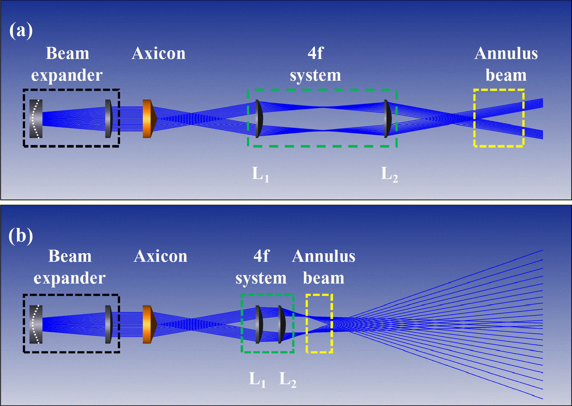
During fs laser fabrication, the profiles of annulus microstructures mainly depend on the relative position of the annulus beam region. In order to better understand the formation of the traditional Bessel annulus beam and improved doughnut beams, the optical simulation software is employed to distinguish the light propagation path of these two different beams, as presented in Fig. 1. These light propagation paths are composed of three convex lenses, a concave lens, and an axicon, the core of which is the axicon. In this Letter, we choose an axicon with an apex angle of 175° from Thorlabs (substrate material, UV fused silica; diameter, 25.4 mm; edge thickness, 5.0 mm). In order to increase readability, we manually expand the cone apex angle without changing the light propagation process in Fig. 1. Otherwise, the 175° axion looks like a biplane cylinder, which will confuse readers. The drawing approach of the convex/concave lens, whose material is K9 silica, is based on the geometric optics principle: the focal length of the lens is equal to half of the radius of curvature. The beam expander in the optical path consists of a concave lens with a focal length of 50 mm and a convex lens of 150 mm, which can collimate the incident Gaussian light and enlarge its diameter to 18 mm. The collimation beam transforms into a Bessel beam after passing through an axicon. Then, we place the system behind the Bessel beam. The system in this Letter consists of two convex lenses with a focal length of 300 mm () and 50 mm (). If the lenses that make up the system are placed at the position of the sum of their focal lengths, the propagation mode of the light path is long and scattered, as shown in Fig. 1(a). If is placed within the focal length of , the propagation mode of light is compact, as shown in Fig. 1(b). In this Letter, we place 85 mm away from within the focal length of . After configuring the position of each lens, we can get the light path shown in Fig. 1.
Figure 1.Shaping optical path of the (a) traditional Bessel annular beam and (b) improved doughnut beam.
Meanwhile, Fig. 2 explains the evolution of the doughnut beam in the yellow dotted box in Fig. 1(b). As shown in Fig. 2, for a doughnut beam shaping optical system, the collimating Bessel area will be focused into an annulus beam with a diameter of by plano-convex lens , which depends on the cone angle of the axicon and focal length of . The relationship between and can be expressed by where is the refractive index of the axicon, is the conic angle, and, if is placed within the focal length of lens as presented in Fig. 2, the diameter of an annulus beam will be reduced to diameter . According to lens imaging and similar triangle principles, the parameter can be calculated as where refers to the distance between where the annulus beam converges and . is the distance of ’s focal plane apart from . is the distance between and .
Figure 2.Schematic diagram for the evolution of the improved doughnut beam.
However, when we use the laser with high processing efficiency and low single-pulse energy (75 kHz, 74.5 μJ), we cannot ablate the copper sheet at the position where the diameter is shown in Fig. 2, since the energy is dispersed on a large diameter annulus. Therefore, the processing region in this Letter is in the annulus region from cross section (a) to cross section (b) with smaller diameters and higher power density behind the annulus region, where the diameter is D, as shown in Fig. 2. We put a sample in the annulus zone, keep and fixed, and then change the axis position of the sample by rotating the Y axis of the 3D platform, which holds the sample to change the diameter of the annulus. We keep the whole optical path system fixed and then move the sample along the optical axis, leading a decreasing trend of the annulus diameter.
Also, the energy distribution in the annulus beam processing region with different diameters was simulated, as shown in Figs. 2(a)–2(d). Therefore, once the distance between lens and is fixed, the annulus beam with different diameters could be obtained by adjusting the position of the sample.
Figure 3 exhibits the schematic diagram of the doughnut beam processing system. The copper was irradiated with a linearly polarized fs laser (Pharos from Light Conversion, Lithuania) with a wavelength of 1030 nm, repetition rate of 75 kHz, and pulse duration of 215 fs. A zero-order half-wave plate is used to vary the laser polarization. An attenuator is used to adjust the laser pulse energy irradiated on the sample surface. Then, the laser beam is transformed into a Bessel beam by an axicon lens with a cone base angle of 2.5°. A lens system consisting of lens and is used to compress the size of the beam and increase the laser intensity at the focal annulus. After passing through the system, the processing annular beam is focused on the front surface of a sample. The sample is mounted on a 3D linear translation stage, which is constituted by three high precision motorized linear stages. The fabrication process is monitored with a charge-coupled device (CCD) camera, through which the morphology of the microstructures could be observed in real time. After irradiation with the shaped fs laser beam, the sample would be placed into an ultrasonic cleaner for 15 min to get rid of recast drips. Finally, the scanning electron microscopy (SEM) and extended depth of field microscopy are utilized to characterize the surface morphology.
Figures 4(a) and 4(b) depict the annulus beam with different diameters at different axial positions calculated by the optical simulation software. In the process of simulation, we set system parameters, including type of incident beam, lens-size unit, and analysis unit, firstly: type of incident beam, Gaussian beam with a wavelength of 1030 nm and beam waist radius of 3 mm; lens-size unit, millimeter; analysis unit, watts per centimeter squared (). Then, we build the beam path model based on the improved doughnut beam path. is placed at a distance away from at 85 mm, and light intensity detectors are placed at intervals of 100 μm in the annulus beam area to detect the light intensity distribution. Meanwhile, there are the annuli processed by a fs laser improved doughnut beam corresponding to the simulation positions, as displayed in Fig. 4(c). Each annulus was fabricated in a single illumination step with certain times controlled by the shutter. The diameter of the annulus is gradually reduced by moving the sample away from the system. The laser pulse energy was 74.5 μJ, and a focusing lens with 50 mm focal length was used in this work. It was observed that the diameters of the fabricated annulus were in good agreement with those of simulated ones. At the same time, we also noticed that the width of the torus obtained by these three experiments was not uniform to some extent, which was mainly caused by the manufacturing error of the cone lens[25].
Figure 4.Calculated annular beam with different diameters at different axial positions in the upper and middle panels, while the fabricated rings corresponding to the simulation positions are in the lower panels.
First of all, the leftmost processing point was set as , the letter M represents the position of the sample on the Y-axis, and the diameter of the annulus obtained at this position is defined as . By constantly moving the sample from the left to the right, a series of annuli with different diameters could be obtained. Under the fixed state of the system, the maximum and minimum diameters that could be processed are 439 μm and 240 μm, respectively. Table 1 shows the measured and calculated diameters and errors at different positions corresponding to the movement. Figure 5 exhibits the relationship between and . All diameter data were mean values by averaging ten measured results each. It is found that the diameter of the fabricated annulus and the movement fit well with the linear function . The points in Fig. 5 are drawn according to the movement amount and experimental amount in Table 1. The blue error bar is drawn according to the error column in Table 1, and the red line is obtained by the linear fitting of the black points in Fig. 5. The equation is obtained by the same linear fitting as the red line.
Movement Amount (μm)
Experimental Diameter (μm)
Simulated Diameter (μm)
Error (%)
0
439
439
2.278
100
421
426
1.663
200
407
407
0.737
300
394
392
0.810
400
372
374
1.613
500
357
359
0.840
600
341
340
0.880
700
326
326
1.840
800
308
309
3.247
900
294
293
1.361
1000
280
276
1.071
1100
260
260
1.154
1200
240
243
2.083
Table 1. Measured and Calculated Diameters and Errors at Different Positions Corresponding to the Movement
Also, the nanostructures laid inside the annulus are characterized. Figure 6 displays the SEM image of the annulus fabricated by improved doughnut beam, where (I) is the processing result obtained without using half-wave plates, and the vertical direction of LIPSSs, shown as the red arrows, represents the initial polarization direction of the polarized laser, and (II) is the processing result after using half-wave plates. The quick axis direction of the half-wave plates is 90° in Fig. 6(a), while the quick axis direction of half-wave plates is 45° in Fig. 6(b). According to the properties of half-wave plates, we know that if the included angle between the vibration direction of the polarized light of the incoming ray, and the fast axis of the wave plate is , then the vibration direction of the polarized light of the output ray turns by in the direction of the fast axis. The blue dotted arrow represents the fast axis direction of half-wave plates, the red arrow is the initial polarization direction of the laser, and the orange arrow is the polarization direction of the linearly polarized laser after passing through the half-wave plates. So, represents the included angle between the vibration direction of the original polarized laser and the fast axis of the half-wave plates, and represents the included angle between the vibration direction of the original polarized light and the vibration direction of the polarized light after passing through the half-wave plates. As is shown in the magnified SEM images of Fig. 6(II) at four different positions (labelled by the angle ), the LIPSSs exhibit as grating-like distributions, the orientations of which are highly uniform and almost perpendicular to the polarization direction at all positions. This phenomenon is attributed to the well-known mechanism of interference and subsequent local field enhancement. As the fast axis direction of half-wave plates goes clockwise from 90° to 45°, the periods of the LIPSSs remain almost unchanged with approximately 700–850 nm, which is significantly lower than the laser wavelength and in agreement with low-spatial-frequency LIPSSs (LSFL) theory[25–27]. To obtain such nanostructures with a Gaussian beam through direct writing by scanning a circle, the orientation of LIPSSs would vary at different positions, which is mostly determined by the writing speed and the angle between the scanning direction and laser polarization. Compared with the common method, the proposed method presents the benefits and advantages of keeping the consistency of the orientation.
Figure 6.SEM images of the rings fabricated by different linearly polarized fs laser improved doughnut beams. (I) The experimental results obtained without adding half-wave plates. The red arrows in the figure represent the initial polarization direction of the laser. (II) The experimental results obtained after adding half-wave plates. The blue dotted arrow represents the fast axis direction of half-wave plates, the red arrow is the initial polarization direction of laser as shown in (I), and the orange arrow is the polarization direction of the linearly polarized laser after passing through the half-wave plates. represents the included angle between the vibration direction of the original polarized laser and the fast axis of the half-wave plates, and represents the included angle between the vibration direction of the original polarized light and the vibration direction of the polarized light after passing through the polarizer.
In addition, the scanned line-widths at different positions are measured for the two annuli. The upper annulus varies in line-width from 12.44 μm to 16.81 μm, while it varies from 13.19 μm to 18.00 μm for the lower annulus. The width of the upper and lower annuli has the same variation trend, which is about 15 μm. According to Zeng’s study[28], the elliptical manufacturing error of the axicon would cause the energy distribution of the annulus diffraction light field to be broken into many bright spots along the annulus, which results in uneven energy distribution at the diffraction ring. This is the main reason for the uneven width of the annulus during the actual machining process.
The most significant advantage of this method is that the diameters of the ring-like focus could be flexibly controlled in a wide range without changing the diameter of the incident light. In our experiments, the distance between the two lenses in the system was fixed, and the obtained axial section of the peak envelope in the processing area was two sides of the isosceles triangle. If we move the position of away from , the base of the isosceles triangle corresponding to the axial section envelope of the peak light intensity will increase, and the processing range will move to the right. This means that the diameters of the fabricated annular microstructures could be continuously changed in a large range if the limitations of laser energy and the aperture of the optical elements meet the requirements.
In summary, an effective method is proposed for the fabrication of annulus micro-/nanostructures by a fs laser improved doughnut beam. Compared with the traditional Bessel annulus beam shaping system, this optical system of improved doughnut beam greatly compresses the light propagation path. According to the simulated and experimental results, it is proved that the obtained axial section of the peak envelope in the processing area is two sides of the isosceles triangle. Also, the diameters of the annulus microstructures could be flexibly adjusted in a wide range by moving the relative position of the sample or the distance between the two lenses in the system. In addition, LIPSSs with controllable direction could be fabricated by this method, which have potential applications in optical antennas.