Abstract
Single layer lattice graphene deposited on the metal substrate can hardly be imaged by the optical microscope. In this Letter, a large field-of-view imaging ellipsometer is introduced to image single layer graphene which is deposited on a metal substrate. By adjusting the polarizer and the analyzer of imaging ellipsometer, the light reflected from surfaces of either single layer graphene or a Au film substrate can be extinguished, respectively. Thus, single layer graphene can be imaged correspondingly under brightfield or darkfield imaging modes. The method can be applied to imaging large-area graphene on a metal substrate.Graphene is used to describe a one-atom thick flat allotrope of carbon, namely a single layer of carbon atoms, which are densely packed into a two-dimensional (2D) hexagonal honeycomb lattice[1–3]. Graphene, a basic building block, can be wrapped up into other different dimensional carbon-based materials, such as zero-dimensional (0D) fullerenes, one-dimensional (1D) nanotubes, and three-dimensional (3D) graphite[2]. There are a variety of methods to prepare graphene, including mechanical cleavage, chemical vapor deposition (CVD), synthesis on SiC, liquid-phase exfoliation, etc[4–8]. Owing to graphene’s diverse properties of high transparency, high strength and elasticity, high electrical and thermal conductivity, low resistance, and so on, it has attracted much attention and had many potential applications in organic light-emitting diodes (OLEDs), transistors, optical modulators, composite materials, energy storage, sensors, biodetectors, fiber lasers, etc[9–12].
Graphene is an important 2D material, and thus it is essential to probe, observe, and image the graphene. To probe the microscopic structure and characterize the graphene layers, a lot of mature methods were often used, such as atomic force microscopy (AFM), transmission electron microscopy (TEM), and Raman spectroscopy[6,13,14]. These probing methods can only investigate the microstructure, e.g. the layer number, and have many shortcomings. AFM has a slow throughput and may cause damage to the graphene’s lattice. For TEM, the graphene consists of only a few identical carbon atoms that interact weakly with the electron beam, and thus TEM needs high acceleration voltages to obtain clear diffraction patterns. For Raman spectroscopy, the differences between two layers and a few layers of graphene are similar and ambiguous in the Raman spectra. In a word, the probing methods mentioned above can only probe the microscopic structure other than the macroscopic properties. For probing graphene’s macroscopic properties, optical microscopy is a useful and convenient way to directly identify and characterize graphene on the substrate in the experiment. The contrast between graphene and the substrate determines whether graphene identification is effective. However, the contrast is usually not high due to the ultrathin graphene ( thickness). Graphene can only be evidently visible, imaged, and characterized by the optical microscope when deposited on a substrate on top of a Si wafer[4,15]. Furthermore, the graphene cannot be visible and imaged by an optical microscope due to the metallic substrate either. In order to extend the optical methods to make single layer graphene deposited on a metal substrate visible and imaged, the imaging ellipsometry is proposed and introduced to observe and image the single layer graphene experimentally.
In our work, an imaging ellipsometer was constructed to observe and image the single layer graphene deposited on Au film[16]. Because the optical constants of graphene and the Au film substrate are different, diverse optical constants result in the fact that the light reflected from either of them can not be extinguished at the same condition in the ellipsometer. Therefore, the different optical constants give contrast between the single layer graphene and the metal substrate. The contrast is the crucial factor for single layer graphene identification and imaging. When the azimuth angles of the polarizer (P), compensator (C), and analyzer (A) are adjusted separately to make the image become increasingly dark, the reflected light beam from both surfaces of graphene and Au substrate cannot be extinguished at the same condition, and then the contrast between them can be recorded by the charge-coupled device (CCD) camera. So, the imaging ellipsometer with a large field of view can characterize and image the single layer graphene deposited on a metallic substrate. In other words, the graphene can be visible and imaged.
Sign up for Chinese Optics Letters TOC. Get the latest issue of Chinese Optics Letters delivered right to you!Sign up now
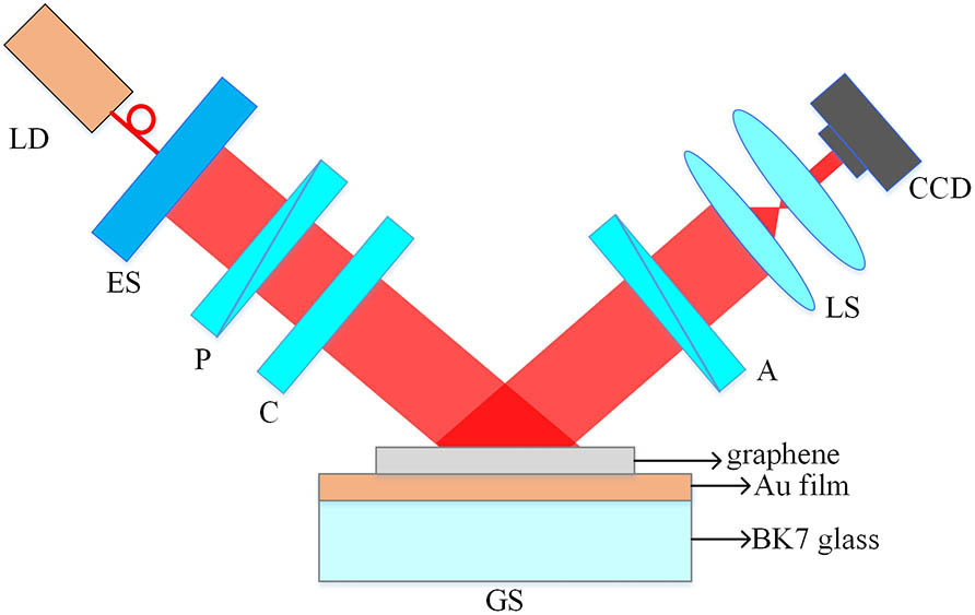
The experimental imaging ellipsometer setup is shown in Fig. 1. The light of the wavelength of 635 nm emitted by a fiber-coupled laser diode (LD) propagates through the expanding system (ES) to expand the cross section of the laser light and collimate the light beam. A P polarizes the incoming light linearly, and later the light becomes an elliptically polarized one after passing through a C. The elliptically polarized light is incident on the graphene sample (GS) and reflected by the sample. The light beam is shaped to a centimeter-sized spot at the sample surface with the incident angle of 45°. So, the imaging ellipsometer is of a large field of view, which is decided mainly by the ES. After passing through an A, the reflected light is collected by a CCD camera. The lens system (LS) is to ensure that the spot size of the light beam can be detected by the CCD camera. The graphene used in our experiment is grown on the copper substrate by CVD and transferred to the 50 nm thick Au film, which is coated on a circular BK7 glass wafer with the diameter of 30 mm. The area of the graphene is .

Figure 1.Schematic diagram of the imaging ellipsometer setup.
The single layer graphene is completely transparent to visible light and cannot be observed and imaged by the optical microscope for most of the substrates which single layer graphene is placed on, such as the metals shown in Figs. 2 and 3. So it is very hard to observe single layer graphene’s macroscopic structure (compared to the atomically microscopic lattice) directly by an optical microscope. As is mentioned above, the single layer graphene deposited on the Au film substrate cannot be viewed and imaged by an optical microscope, and the corresponding experimental images of the GS on the Au film substrate are illustrated in Figs. 2 and 3. The GS was observed in an Olympus BX51 optical microscope under normal white-light illumination on top of the sample. The GS is viewed under a objective lens. In order to ensure the results’ accuracy, all of the images collected in Fig. 2 are obtained under a conventional light microscope and a polarized light microscope, respectively. For both conventional and polarized light microscopes, the graphene deposited on the Au film substrate cannot be distinguished from the substrate. It proves experimentally that the graphene on the Au substrate cannot be visible and imaged by optical microscopy.
Figure 2.Experimental images of two different places on the graphene sample surface captured by a conventional light microscope.
Figure 3.Experimental images of two different places on the graphene sample surface captured by a polarized light microscope.
Compared to the disabled observation of the GS on the Au film substrate, the GS can be distinguished and imaged by the large field-of-view imaging ellipsometer, as is demonstrated in Fig. 4. Owing to the different optical constants of graphene and Au film substrate, the reflected light beams from their surfaces cannot be extinguished at the same time when the P, C, and A are adjusted separately. If one of the light beams is extinguished, another is still there, and the difference between them becomes obvious and can be imaged. Figures 4(a) and 4(b) show that the reflected light from the graphene surface is extinguished, and the graphene area can be easily recognized and imaged. In other words, the graphene deposited on the Au substrate gets imaged under the imaging ellipsometer.
Figure 4.Experimental images of two different places on the graphene sample under the brightfield imaging mode with the reflected light from the graphene surface extinguished and captured by the large field-of-view imaging ellipsometer.
In order to be compared with the optical microscope, both the brightfield and darkfield imaging modes were discussed. For convenience, the azimuth of the C is set to 45°, and thus adjusting the P and A is enough to make the reflected light from either graphene or the Au film substrate be extinguished in the experiment, respectively, which corresponds to brightfield and darkfield imaging modes, respectively. In fact, for the same place on the sample surface, the graphene can always be visible and imaged when the reflected light is extinguished from the surface of either graphene or the Au film substrate, as is illustrated in Figs. 5(a) and 5(b), corresponding to brightfield and darkfield imaging modes, respectively. What is more, the imaging ellipsometer can be used to observe and image the GS on the metal substrate with a large area because the light spot becomes centimeter-sized at the sample surface and can be scalable.
Figure 5.Experimental images of the same place on the graphene sample under the large field-of-view imaging ellipsometer captured under (a) brightfield and (b) darkfield imaging modes with the reflected light from surfaces of (a) graphene and (b) Au film substrate extinguished, respectively.
In summary, the imaging ellipsometry is introduced to observe and image graphene on a metal substrate, and the method proves to be effective and convenient. Through adjusting the P and A of the imaging ellipsometer, the graphene deposited on the Au film substrate can be visible and imaged when the light from surfaces of either graphene or the Au film substrate is extinguished. Further, the imaging ellipsometer can be applied for imaging graphene on a metal substrate with a large area due to its large field of view. Some few-layer graphene resembles the single layer lattice, and further experiments will be conducted on imaging and measuring multilayer differences from the single layer lattice.
References
[1] K. S. Novoselov, A. K. Geim, S. V. Morozov, D. Jiang, M. I. Katsnelson, I. V. Grigorieva, S. V. Dubonos, A. A. Firsov. Nature, 438, 197(2005).
[2] A. K. Geim, K. S. Novoselov. Nat. Mater., 6, 183(2007).
[3] A. K. Geim. Science, 324, 1530(2009).
[4] K. S. Novoselov, D. Jiang, F. Schedin, T. J. Booth, V. V. Khotkevich, S. V. Morozov, A. K. Geim. Proc. Natl. Acad. Sci. U. S. A., 102, 10451(2005).
[5] T. Ohta, A. Bostwick, T. Seyller, K. Horn, E. Rotenberg. Science, 313, 951(2006).
[6] Y. Hernandez, V. Nicolosi, M. Lotya, F. M. Blighe, Z. Y. Sun, S. De, I. T. McGovern, B. Holland, M. Byrne, Y. K. Gun’ko, J. J. Boland, P. Niraj, G. Duesberg, S. Krishnamurthy, R. Goodhue, J. Hutchison, V. Scardaci, A. C. Ferrari, J. N. Coleman. Nat. Nanotechnol., 3, 563(2008).
[7] K. S. Kim, Y. Zhao, H. Jang, S. Y. Lee, J. M. Kim, K. S. Kim, J. H. Ahn, P. Kim, J. Y. Choi, B. H. Hong. Nature, 457, 706(2009).
[8] X. S. Li, W. W. Cai, J. H. An, S. Kim, J. Nah, D. X. Yang, R. Piner, A. Velamakanni, I. Jung, E. Tutuc, S. K. Banerjee, L. Colombo, R. S. Ruoff. Science, 324, 1312(2009).
[9] K. S. Novoselov, V. I. Fal’ko, L. Colombo, P. R. Gellert, M. G. Schwab, K. Kim. Nature, 490, 192(2012).
[10] Y. K. Yap, R. M. De La Rue, C. H. Pua, S. W. Harun, H. Ahmad. Chin. Opt. Lett., 10, 041405(2012).
[11] H. Ahmad, F. D. Muhammad, M. Z. Zulkifli, S. W. Harun. Chin. Opt. Lett., 11, 071401(2013).
[12] P. Tang, Y. Tao, Y. Mao, M. Wu, Z. Huang, S. Liang, X. Chen, X. Qi, B. Huang, J. Liu, C. Zhao. Chin. Opt. Lett., 16, 020012(2018).
[13] C. N. R. Rao, A. K. Sood, K. S. Subrahmanyam, A. Govindaraj. Angew. Chem. Int. Ed., 48, 7752(2009).
[14] A. C. Ferrari, J. C. Meyer, V. Scardaci, C. Casiraghi, M. Lazzeri, F. Mauri, S. Piscanec, D. Jiang, K. S. Novoselov, S. Roth, A. K. Geim. Phys. Rev. Lett., 97, 4(2006).
[15] P. Blake, E. W. Hill, A. H. Castro Neto, K. S. Novoselov, D. Jiang, R. Yang, T. J. Booth, A. K. Geim. Appl. Phys. Lett., 91, 063124(2007).
[16] L. Y. Gu, A. J. Zeng, S. Y. Hu, Q. Yuan, W. L. Cheng, S. H. Zhang, G. H. Hu, H. B. He, H. J. Huang, 10023, 1002315(2016).