Abstract
Surface channel waveguides (WGs) were fabricated in a monoclinic crystal by femtosecond direct laser writing (fs-DLW). The WGs consisted of a half-ring cladding with diameters of 50 and 60 μm located just beneath the crystal surface. They were characterized by confocal laser microscopy and -Raman spectroscopy, indicating a reduced crystallinity and stress-induced birefringence of the WG cladding. In continuous-wave (CW) mode, under Ti:sapphire laser pumping at 802 nm, the maximum output power reached 171.1 mW at 1847.4 nm, corresponding to a slope efficiency of 37.8% for the 60 μm diameter WG. The WG propagation loss was . The top surface of the WGs was spin-coated by a polymethyl methacrylate film containing randomly oriented (spaghetti-like) arc-discharge single-walled carbon nanotubes serving as a saturable absorber based on evanescent field coupling. Stable passively -switched (PQS) operation was achieved. The PQS 60 μm diameter WG laser generated a record output power of 150 mW at 1846.8 nm with . The conversion efficiency with respect to the CW mode was 87.6%. The best pulse characteristics (energy/duration) were 105.6 nJ/98 ns at a repetition rate of 1.42 MHz.1. INTRODUCTION
Waveguide (WG) lasers emitting in the spectral range of are of interest for bio- and environmental sensing applications. This is because such a radiation matches spectrally with the absorption of some relevant molecules, such as or . Typically, laser emission at is achieved using thulium () or holmium () ions. In the former case, the emission is due to the transition [1]. ions are attractive because of a strong absorption at ( transition), efficient cross-relaxation (CR) enhancing the pump quantum efficiency up to 2 [2], low-threshold behavior, and typically large Stark splitting of the ground state leading to a broadband tuning feature.
Highly efficient laser operation was achieved with continuous-wave (CW) Tm WG lasers. In Ref. [3], a “mixed” crystalline channel WG laser generated 1.6 W at 1.84 μm with a record slope efficiency of 80%, promoted by an efficient CR at a high doping level. The active layer was fabricated by liquid phase epitaxy (LPE) [4]. The WG propagation loss was [5]. The refractive index contrast with respect to the undoped substrate was . Note that the active material belongs to the crystal family of monoclinic double tungstates (DTs), which are well-known for ion doping due to their advantageous spectroscopic properties for polarized light [6].
Another method of fabricating photonic microstructures in transparent dielectric materials has attracted a lot of attention, namely femtosecond direct laser writing (fs-DLW) [7–10]. This method is easier than LPE or pulsed laser deposition [11] and it allows for three-dimensional (3D) WG geometries. It can be applied to a variety of glass and crystalline materials. To date, several studies have been dedicated to CW fs-DLW Tm WG lasers [12–17]. One can note the results achieved in Ref. [16] with an fs-DLW Tm:ZBLAN glass channel WG laser, which generated 205 mW at 1.89 μm with (corresponding to ).
Sign up for Photonics Research TOC. Get the latest issue of Photonics Research delivered right to you!Sign up now
Recently, we employed fs-DLW for the fabrication of depressed-index buried channel WGs in -doped monoclinic DTs. In Ref. [18], proof of the concept was demonstrated using a bulk (shortly Tm:KLuW) crystal, and circular-cladding channel WGs were prepared. Power scaling of such lasers was shown in Ref. [19] using a hexagonal lattice-like cladding WG. The output power reached 136 mW at 1.844 μm with , and the WG propagation loss was estimated to be 1.2 dB/cm. The spatially averaged variation of the negative refractive index change across the microstructured cladding was .
Passive -switching is a commonly used method to produce nanosecond (ns) pulses in solid-state lasers. It is typically realized by the insertion into the cavity of a nonlinear optical element—a saturable absorber (SA) whose linear absorption spectrally matches the laser wavelength.
Recently, multiple studies were dedicated to novel nanostructured SAs featuring a broadband linear and saturable absorption due to the special band structure. The most prominent example is carbon nanostructures, such as graphene [20,21], representing a 2D layer of carbon atoms arranged in a honeycomb lattice, and single-walled carbon nanotubes (SWCNTs) [22], representing rolled sheets of graphene. Other materials, such as few-layer transition metal dichalcogenides [23,24] (e.g., , , or ), topological insulators, and related nanomaterials (e.g., , , or ) [25–27], black phosphorus [28], graphene oxide [29], and graphite nanoparticles [30], were also studied.
SWCNTs are promising SAs for passively -switched (PQS) solid-state lasers at 2 μm as they offer low saturation intensity, high fraction of saturable losses, and ultrafast recovery time of initial absorption. The fabrication of a SWCNT-SA is relatively easy. SWCNTs provide compatible pulse characteristics as compared to, for instance, commercial semiconductor SAs for 2 μm [31]. SWCNTs have been employed in PQS compact microchip-type (thermally guided) Tm lasers. In Ref. [32], an SWCNT PQS Tm:KLuW laser generated 25 ns/1.1 μJ pulses at a repetition rate of 0.64 MHz.
To date, only a few studies have been dedicated to PQS Tm WG lasers leading either to long (few μs) pulses or low average output power (few mW) [33–37]. Such SAs as , graphene, topological insulator (), and SWCNTs were studied. For instance, in Ref. [36], an fs-DLW Tm:ZBLAN glass WG laser PQS by graphene generated 2.8 μs/240 nJ pulses at an output power of only 6 mW. Very recently, we employed SWCNTs in an fs-DLW Tm:KLuW WG laser providing much shorter pulses (50 ns/7 nJ) while the output power was still low, 10.3 mW [18].
The feature of the previously studied PQS Tm WG lasers was the use of transmission-type SAs. It is known that in such a geometry the SA suffers from heating due to the residual pump, causing -switching intensity instabilities and even laser-induced damage [21]. The interaction length (modulation depth) is limited by the SA thickness. On the other hand, an increase of the thickness will lead to higher insertion loss and lower laser efficiency. An alternative method is the deposition of the SA on top of a surface WG laser, so that the saturation of the SA is provided by an indirect interaction with the exponentially decaying evanescent field extending into the cladding along the propagation length. This method allows one to increase the interaction length with the SA, avoid its heating, and reduce the insertion losses. It is well known and has been extensively studied at in WG lasers based on and ions [38–42]. SWCNTs have also been employed in this WG laser geometry. In Ref. [38], a planar WG laser generated 433 ns/110 nJ pulses at a repetition rate of 0.23 MHz. Note that particularly surface channel WG lasers are of interest for evanescent-field-interaction SA -switching as their top surface can be easily functionalized. Evanescent-field-interaction SAs have also been successfully implemented in mode-locked fiber lasers [43,44].
In the present work, we aimed to demonstrate passive -switching of a Tm surface waveguide laser based on evanescent field coupling operating in the 2 μm spectral range. We used a -doped monoclinic DT crystal as a gain material, fs-DLW for the preparation of the WGs, and SWCNTs as an SA. The proposed geometry allowed us to achieve a record output power for any PQS Tm WG laser.
2. FABRICATION OF THE WAVEGUIDES
A. Femtosecond Direct Laser Writing
Depressed-index surface channel WGs were fabricated in a bulk Tm:KLuW crystal by fs-DLW. The active crystal was grown by the top-seeded-solution growth slow-cooling method using as a solvent [6]. It was doped with 3 at. % (). Tm:KLuW is monoclinic (sp. gr. ) and optically biaxial. A rectangular sample was cut for light propagation along the optical indicatrix axis, because it gives access to the high-gain polarization and corresponds to athermally compensated thermo-optic properties [45]. The sample thickness was 3.4 mm. Its aperture was , and both faces were polished to laser-grade quality and remained uncoated. Before the DLW and deposition of the SA, the two faces were also polished to a laser-grade quality using a Logitech PM5 polishing machine and alumina powders in the range of 9–0.3 μm in diameter. When inspecting such surfaces with atomic force microscopy (Pico SPM II), we observed no defects, and the root-mean-square (rms) surface roughness was about .
The DLW was performed using 120 fs, 795 nm pulses from a Ti:sapphire regenerative amplifier (Spitfire, Spectra Physics) employing a small amount of the pulse energy at 1 kHz repetition rate. The laser beam was focused into the crystal with a microscope objective (numerical aperture, ). The fraction of the pulse energy incident on the crystal was 65 nJ. The crystal was scanned at a speed of 500 μm/s along its -axis, producing the damage tracks. The polarization of the fs laser was perpendicular to the writing direction (). The line scan procedure was repeated at different depths and lateral positions of the crystal to make half-ring-shaped cladding structures. Two surface channel WGs with core diameters of 50 and 60 μm were fabricated. Each cladding consisted of a total of 31 and 45 damage tracks, respectively. The separation between adjacent tracks along the horizontal direction was 2 μm. The axes of the waveguides were located at 25 μm beneath the crystal surface. Typical cross-section sizes of inscribed tracks were of 600 nm in width and 6 μm in height as previously observed in crystalline cladding waveguides fabricated in the same experimental conditions [46].
The selection of 50 and 60 μm diameter WGs is due to low propagation losses (below 1 dB/cm) expected for such structures according to our previous experiments.
B. Coating with SWCNTs
The commercially available SWCNTs (Meijo Nano Carbon Co., Ltd.) were synthesized by the arc-discharge method. They had diameters varying from 1.5 to 2.2 nm. The SWCNTs were dissolved in 1,2-dichlorobenzene (o-DCB) at concentrations of 0.1–0.35 mg/mL and agitated in an ultrasonic bath. The SWCNT solution was centrifuged for about 20 min to induce sedimentation of large bundles and metal impurities. The well-dispersed SWCNT solution was then mixed with a separately prepared polymethyl methacrylate (PMMA, Polymer Source, Inc.) solution (100 mg/mL in o-DCB) at a volume ratio of 1:1 and stirred. The final concentration of SWCNTs in PMMA was 0.1–0.35 wt. %.
To fabricate the evanescent-field coupled SA, the 0.35 wt. % SWCNT/PMMA film was spin-coated on the top surface of the Tm:KLuW crystal containing the WGs. The whole length of the WGs was covered with the film. The WG faces were protected during the spin-coating. For the measurements of transmission spectra, films with different SWCNT concentrations were spin-coated on uncoated quartz substrates. The coated samples were placed on a hot plate in a vacuum oven to dry the SWCNT/PMMA film. The individual nanotubes were randomly oriented in the films (spaghetti-like); see Ref. [32] for scanning electron microscopy images of SWCNTs. The spin-coating speed was 1500 r/min. All deposited films had a thickness of 300 nm. More details can be found elsewhere [22,32]. Note that in Ref. [22], high-pressure carbon monoxide (Technique) SWCNTs were used, but the fabrication procedure was similar.
The deposited films were clear and uniform and contained no particles as examined by optical microscopy. The small-signal transmission () spectra of the SWCNT/PMMA films deposited on quartz substrates are shown in Fig. 1(a) (the Fresnel losses are subtracted). For the same film thickness, it was possible to vary the absorption by changing the concentration of SWCNTs. The films feature a broadband absorption at 1.6–2.2 μm due to the first fundamental transition of the semiconducting nanotubes (). For the 0.35 wt. % SWCNT/PMMA film, at 1.85 μm (small-signal absorption ). Note that the film thickness can be changed by varying the spin-coating speed (1500–200 r/min) and the number of coating runs (1–3).
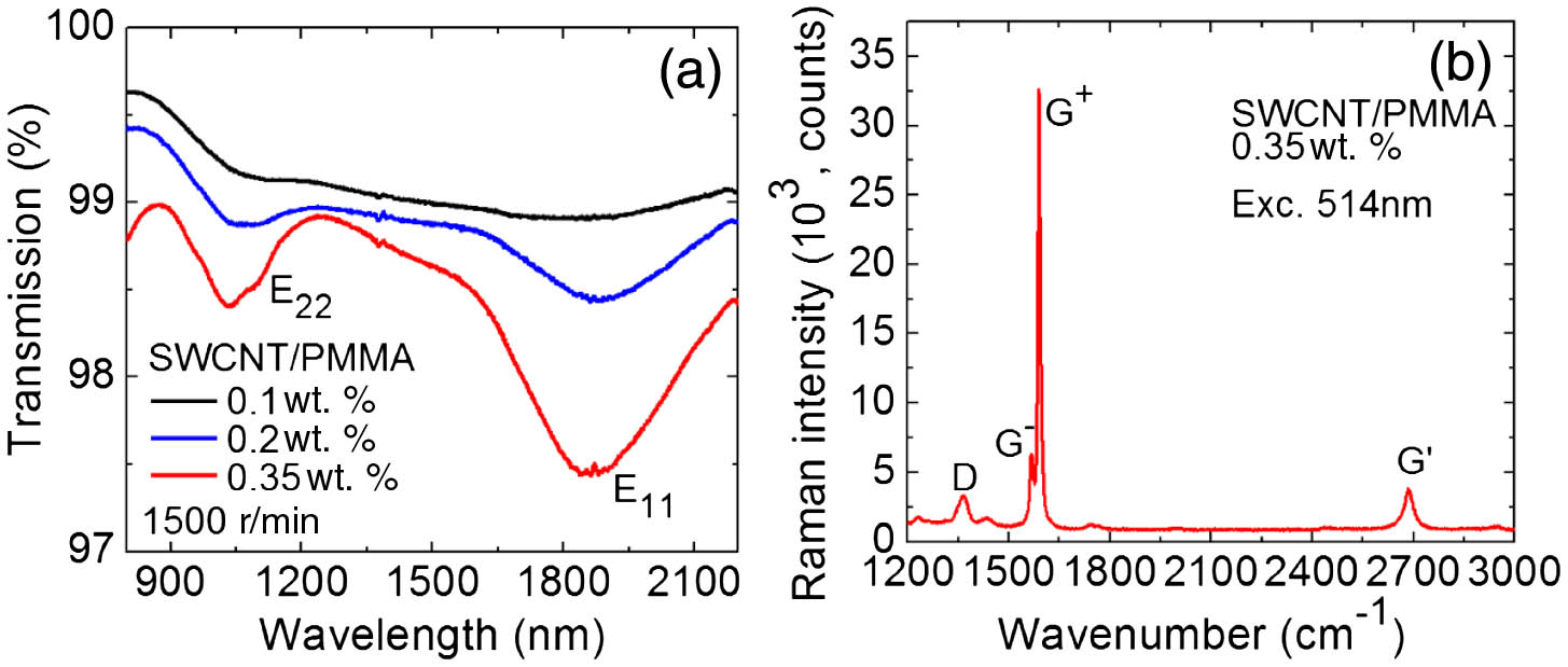
Figure 1.(a) Small-signal internal transmission spectra of the SWCNT/PMMA films coated on quartz substrates with different concentrations of SWCNTs (0.1–0.35 wt. %); the spin-coating speed is 1500 r/min. (b) Raman spectrum of the 0.35 wt. % SWCNT/PMMA film coated on the surface of Tm:KLuW, .
Raman spectra were measured for the 0.35 wt. % SWCNT/PMMA film spin-coated on the Tm:KLuW WGs; see Fig. 1(b). The excitation wavelength was 514 nm (-ion laser). The most intense G-band is the optical phonon mode of graphite materials. This band is split, which is a distinctive feature of cylindrically rolled graphene sheets, that is, SWCNTs. The high-frequency peak () corresponds to vibrations of C atoms along the nanotube axis, and the low-frequency one () arises from vibrations along the circumferential direction. The other bands are assigned as and . The radial beating mode (160–190 cm−1, as determined using films coated on quartz substrates) was not resolved because it overlaps with strong Raman bands of KLuW crystal.
The absorption saturation property of SWCNT/PMMA films was proved by pump-probe experiments at 1.92 μm, revealing two characteristic recovery times , “fast” (0.25 ps) and “slow” (1.16 ps) [47]. The saturation intensity of a similar SWCNT-based transmission-type SA was estimated as and the fraction of the saturable losses as 0.21 at [32].
Optical microscope images of the SWCNT/PMMA film and the top surface of the Tm:KLuW crystal coated with this film are shown in Fig. 2.

Figure 2.(a) Optical microscope image of the surface of SWCNT/PMMA film ( magnification); (b) photograph of the Tm:KLuW crystal containing surface channel WGs with the deposited SWCNT/PMMA film.
3. CHARACTERIZATION OF THE WAVEGUIDES
A. Confocal Laser Microscopy
First, we studied the WGs by confocal laser microscopy using an LSM 710 microscope (Carl Zeiss) equipped with a polarizer (), an analyzer (), a blue GaN laser (405 nm), and an ion laser (488 nm). The characterization started with one of the laser-grade-polished end-faces of the WGs; see Fig. 3. The measurements were done in transmission mode with polarized light ().
Figure 3.Confocal laser microscopy of a polished end-face of the fs-DLW Tm:KLuW surface channel WGs with cladding diameters of (a) 60 μm and (b) 50 μm, transmission mode, polarized light (), .
A clear dark half-ring of damage tracks having a length of 6 μm is observed. The surrounding bulk crystal does not contain any cracks. The inner part of the WG is darker because part of the light is coupled and is not detected.
Then the polished top-surface of the WGs (before the SWCNT coating) was also examined using the transmission mode. With polarized light (), a dark half-barrel-shaped cladding is surrounded by the bright unmodified bulk material; see Figs. 4(a) and 4(b). The cladding has a periodic net-like surface. With crossed polarizers (), a bright cladding is seen in the dark crystal, Figs. 4(c) and 4(d). For crossed polarizers oriented along the optical indicatrix axes of KLuW, no transmitted light is expected for the stress-free bulk crystal. A modification of the cladding may provide an additional phase shift due to the stress-optic effect, leading to transmission of light through the crossed and . Figures 4(c) and 4(d) indicate such a birefringence of the cladding.
Figure 4.Confocal laser microscope images (top view) of the central part of the half-ring cladding fs-DLW surface WGs in Tm:KLuW: (a), (b) transmission mode, polarized light (), ; (c), (d) transmission mode, crossed polarizers (, ), . WGs: (a), (c) 60 μm cladding and (b), (d) 50 μm cladding.
B. μ-Raman Spectroscopy
The modification of the crystal structure in the WG core and cladding regions was further studied with -Raman mapping spectroscopy. A Renishaw inVia Reflex microscope with a 514 nm ion laser and a Leica microscope objective was used. The excitation laser was linearly polarized with in the crystal. The measurement geometry was . We monitored the most intense internal Raman mode at related to the W–O stretching vibrations in the distorted octahedra of KLuW [6]. Its peak intensity and position were studied over the cross section of the WG faces with a spatial resolution of 0.4 μm.
The results are shown in Fig. 5. Both the Raman peak intensity and the peak frequency (in ) are similar in the WG core volume and in the pristine bulk crystal surrounding the WG. Thus, the crystalline quality of the material in the core region is preserved. A reduction of the Raman peak intensity and a phonon energy shift of to higher frequencies are observed in the cladding region. These changes indicate a reduced crystallinity of the damaged material within the cladding, as well as the presence of microstress-induced lattice compaction leading to higher phonon energy, both agreeing well with the presence of depressed index changes at tracks as well as collateral induced stress fields.
Figure 5.-Raman mapping of a lateral face of the fs-DLW Tm:KLuW surface channel WGs monitoring the Raman band: (a), (c) peak intensity (a.u.) and (b), (d) peak frequency (). WGs: (a), (b) 60 μm cladding and (c), (d) 50 μm cladding. The measurement geometry is . The -axis is horizontal.
4. LASER SETUP
The scheme of the laser setup is shown in Fig. 6. The fs-DLW waveguide laser was pumped by a CW Ti:sapphire laser (MIRA 900, Coherent) tuned to . The polarization of the pump beam corresponded to in the WG. It was coupled into the waveguides with a microscope objective (, focal length ) resulting in a spot radius of 20 μm at the focus located at the front end-face of the WG. The incident pump power was varied with a gradient neutral density (ND) filter. Under 802 nm pumping, the WGs exhibited blue (480 nm) upconversion luminescence ( transition of ).
Figure 6.(a) Scheme of the PQS fs-DLW Tm:KLuW surface WG laser: ND, gradient neutral density filter, PM, pump mirror, WG, waveguide, OC, output coupler, F, cutoff filter. (b) Photograph of the Ti:sapphire pumped WG showing blue upconversion luminescence.
The Tm:KLuW sample containing the fs-DLW WGs was placed on a passively cooled Al support. The laser cavity consisted of a flat pump mirror which was antireflection coated for 0.7–1.0 μm and high-reflection coated for 1.8–2.1 μm and a flat output coupler (OC) having a transmission of 1.5%, 3%, 5%, 9%, 20%, and 30% at 1.8–2.1 μm. The PM and the OC were placed close to the WG endfaces with minimum air gaps. No index-matching liquid was used. The physical cavity length was then 3.4 mm.
The pump absorption under lasing conditions, , and the coupling efficiency, , were determined from a combination of pump-transmission studies at 802 and at 830 nm (out of the absorption) and a rate-equation modelling accounting for the bleaching of the ground-state () and CR for the ions [48]. was for both WGs, and amounted to , depending on the OC. Note that the small-signal pump absorption calculated from the spectroscopic data is ( is the corresponding absorption cross-section of ions in KLuW for ) [6].
The laser output was collimated using an uncoated lens with . The nonabsorbed pump was blocked using a long-pass filter (FEL 1000, Thorlabs). The output power was measured with an Ophir Nova P/N 1Z01500 power meter. The real output was corrected for the optical losses at the lens and filter. The emission spectrum was measured using an optical spectrum analyzer (AQ6375B, Yokogawa). Imaging of the waveguide laser near-field output mode at 1850 nm wavelength was performed using a FIND-R-SCOPE near-IR camera (model 85726). The laser mode size at the output face of the WG was calibrated using a 1951 USAF resolution test target (R1DS1, Thorlabs). The oscilloscope traces were detected using a fast InGaAs photodiode and a 2 GHz Tektronix DPO5204B digital oscilloscope.
5. RESULTS AND DISCUSSION
A. CW Operation
Before the SWCNT/PMMA coating of the WGs, we studied their CW performance. The corresponding input–output dependences are shown in Fig. 7. The laser emission was linearly polarized, (horizontal). The polarization was naturally selected by the anisotropy of the gain. The output dependences were linear for all OCs up to at least of absorbed pump power (), indicating the lack of detrimental thermal effects. No damage of the WGs was observed.
Figure 7.Input–output dependences for CW fs-DLW Tm:KLuW surface channel WG lasers with (a) 60 μm and (b) 50 μm cladding, –slope efficiency. The laser polarization is .
The 60 μm WG exhibited the best laser performance, Fig. 7(a). For the optimum 30% OC, the maximum CW output power was 171.1 mW at 1847.4 nm corresponding to a slope efficiency of 37.8% (with respect to ). The laser threshold was as low as 52 mW. For the 50 μm WG, a lower output power of 150.6 mW at 1847.2 nm and lower of 34.5% were achieved, Fig. 7(b). The laser threshold increased to 59 mW (for the same ). For both WGs, the laser performance improved with indicating a minor effect of upconversion that is known to affect the laser performance of -doped materials at high inversion rates associated with high output coupling.
The achieved CW output power and the slope efficiency exceed the values reported previously for the hexagonal-cladding fs-DLW buried Tm:KLuW WG [19].
The typical laser emission spectra for both CW WG lasers are shown in Fig. 8 (measured at maximum ). With the increase of output coupling from 1.5% to 30%, the emission shifted to shorter wavelengths. This behavior is due to the quasi-three-level nature of ions, and it is related to an increase of (in other words, a decrease of reabsorption) with . For the 60 μm WG, the laser wavelength blueshifted from 1947.4 to 1847.4 nm and for the 50 μm WG, from 1916.4 to 1847.2 nm.
Figure 8.Typical laser emission spectra of CW fs-DLW Tm:KLuW surface channel WG lasers with (a) 60 μm and (b) 50 μm cladding (measured at maximum , Fig. 4). The laser polarization is .
For the two studied WGs, the laser oscillations occurred around two narrow spectral ranges. For the 60 μm WG, the laser emitted at for small and at for higher output coupling. For the 50 μm WG, the emission was at for small , in two spectral ranges for intermediate 3%–5% output coupling, and finally for it was solely at . This is related to the presence of three narrow local peaks in the gain spectra of ions in KLuW for [6]. The prevalence of these peaks is changing with .
The WG propagation loss was estimated from a Caird analysis modified for high output coupling [17], , where and , is an internal loss per pass, and is an intrinsic slope efficiency. Figure 9 shows a plot of the inverse of the slope efficiency versus the inverse of the outcoupling loss for both WGs. The least-square fit of the experimental data yields , for the 60 μm WG and , for the 50 μm one. These values of the WG propagation loss are lower than those reported for an fs-DLW Tm:KLuW WG with a hexagonal cladding (1.2 dB/cm) [19] and for an fs-DLW WG based on a pair of damage tracks (1.9 dB/cm) [49] and indicate the good potential of the designed structures for further PQS experiments.
Figure 9.Modified Caird analysis for 60 and 50 μm cladding CW fs-DLW Tm:KLuW surface channel WG lasers (symbols: experimental data; lines: their linear fits).
A higher propagation loss for the 50 μm WG explains its worse laser performance—see Fig. 7(b)—namely, lower and higher laser threshold, as well as shorter laser wavelengths achieved even with smaller , Fig. 8(b), as compared with the 60 μm WG.
The measured intensity spatial profiles of the output laser mode for CW fs-DLW Tm:KLuW surface WG lasers are shown in Figs. 10(a) and 10(b). The laser mode was confined by the half-ring-shaped cladding from below and the air–sample interface from above. Because of this, the mode profiles were slightly asymmetric, and they were extended in the vertical direction (-axis). For both directions, and , the intensity profiles were well fitted with a Gaussian function; see Figs. 10(c) and 10(d). No notable change of the beam profiles with was observed.
Figure 10.Spatial near-field beam profiles of the output laser mode from the CW fs-DLW Tm:KLuW surface channel WG lasers with (a), (c) 60 μm and (b), (d) 50 μm cladding, , . The profiles were calibrated with respect to the WG output end-face. (a), (b) 2D profiles, (c), (d) intensity plots along the directions of the axis (horizontal) and the axis (vertical). Symbols: experimental data; curves: their Gaussian fits.
Using the calibration target, we determined the actual size of the laser mode at the output end-face of both WGs. For the 60 μm one, the mode diameters were 58.3 μm (horizontal, ) and 62.8 μm (vertical, ). For the 50 μm WG, was smaller, 48.1 μm (horizontal), and 52.3 μm (vertical). Thus, the measured mode was mostly confined inside the WG cladding and the size of the mode follows the spatial shape and size of the cladding structures.
Finite element method numerical simulations of the waveguides incorporating various index change processes (damage and stress-optic index changes) have also been performed. Such simulations allow us to predict local index change values at submicrometer volumes within the cladding region at the near-IR range. The simulations of the waveguides, following our previous simulation model (see Ref. [46] for further results), deliver fundamental modes for both waveguides very similar to those measured, Fig. 11. The obtained refractive index change at submicrometer tracks is of , which are values very similar to those previously obtained for fs-DLW channel WGs fabricated under the same laser conditions but on crystals [46].
Figure 11.Simulated fundamental mode for (a) 60 μm and (b) 50 μm WG. The DLW tracks and the crystal surface are indicated by red color. The assumed refractive index change at DLW tracks is .
B. Passive Q-Switching
After the CW laser experiments, the WGs were spin-coated with the SWCNT/PMMA film. The coated Tm:KLuW sample was tested in the same laser setup. Two OCs with transmission of 20% and 30% were used. Stable passive -switching was achieved with both WGs and OCs. In all cases, the laser output was linearly polarized, . No damage of the sample or SA was observed after a long-term, about an hour, operation. No special laser alignment was needed to observe -switching.
The input–output dependences are shown in Fig. 12(a). They were linear for both OCs up to at least . The 60 μm WG laser provided the best output performance. For , it generated a maximum average output power of 150 mW at 1846.8 nm with . Considering the output power achieved in the CW mode, the -switching conversion efficiency was as high as 87.6%. Note that a small blueshift of the emission wavelength with respect to the CW laser, Fig. 8(a), and a very high indicate low insertion loss for the SWCNT-SA. For the same OC, the 50 μm WG laser emitted a lower average output power of 115 mW at a slightly shorter wavelength of 1844.0 nm with and .
Figure 12.fs-DLW Tm:KLuW surface channel WG lasers PQS by evanescent-field coupling with SWCNT-SA: (a) input–output dependences, is slope efficiency; (b) typical laser emission spectra measured at maximum . The laser polarization is .
The typical emission spectra of the PQS WG lasers are shown in Fig. 12(b). With increasing , the spectra experienced a slight blue shift, e.g., from 1847.9 to 1846.8 nm for the 60 μm WG. For all studied WGs and OCs, the laser oscillations were around 1.85 μm.
The pulse characteristics, such as the pulse repetition frequency (PRF) and pulse duration (determined as full width at half-maximum, FWHM) were measured directly. The pulse energy was calculated from the average output power as , and the peak power as . The results on the pulse characteristics obtained with the optimum are shown in Fig. 13. All of them were dependent on . This effect is known for “fast” SAs such as graphene and SWCNTs, and it is related to the dynamic bleaching of the SA [50].
Figure 13.Pulse characteristics of fs-DLW Tm:KLuW surface channel WG lasers PQS by evanescent-field coupling with SWCNT-SA: (a) pulse duration, (b) PRF, (c) pulse energy, and (d) peak power. .
For the 60 μm WG laser with the increase of from 0.1 to 0.5 W, the pulse duration shortened from 237 to 98 ns, the pulse energy increased from 24 to 105.6 nJ, and the PRF increased from 0.86 to 1.42 MHz. The maximum peak power reached 1.07 W. For the 50 μm WG laser, the best pulse characteristics were 52.2 nJ/90 ns at a PRF of 2.20 MHz. The maximum value was 0.58 W.
The oscilloscope traces of the shortest single -switched pulses and the corresponding pulse trains recorded at the maximum of 0.5 W (for both studied WG lasers) are shown in Fig. 14. The single -switched pulses have a nearly Gaussian temporal shape. The intensity instabilities in the pulse trains are , and the root mean square (rms) pulse-to-pulse timing jitter is (for both WGs).
Figure 14.Oscilloscope traces of (a), (b) the typical pulse trains and (c) the corresponding single -switched pulses for the fs-DLW Tm:KLuW surface channel WG lasers PQS by evanescent-field coupling with SWCNT-SA. WG lasers with (a), (c) 60 μm and (b), (c) 50 μm cladding, , .
The output characteristics of the fs-DLW Tm:KLuW surface channel WG lasers PQS by SWCNTs are listed in Table 1.
| WG | TOC | Pout, mW | λL, nm | η,% | ηconv,% | Δτ, ns | Eout, nJ | PRF, MHz |
| 60 μm | 30% | 150 | 1846.8 | 34.6 | 87.6 | 98 | 105.6 | 1.42 |
| 20% | 141 | 1847.9 | 30.9 | 86.5 | 96 | 94.6 | 1.49 |
| 50 μm | 30% | 115 | 1844.0 | 24.6 | 76.3 | 90 | 52.2 | 2.20 |
| 20% | 85 | 1846.6 | 21.0 | 75.2 | 111 | 58.2 | 1.46 |
Table 1. Pulse Characteristics of the fs-DLW Tm:KLuW Surface Channel Waveguide Lasers PQS by Evanescent-Field Coupling with SWCNTs
The results achieved in the present work represent the highest average output power (150 mW) and slope efficiency (34.6%) ever achieved in any PQS Tm waveguide laser. We refer this to the use of a surface-deposited SA, thus minimizing the insertion losses, as indicated by the high achieved -switching conversion efficiency of 87.6%. The shortest pulses (50 ns) from a PQS Tm waveguide laser were obtained in Ref. [18] using a buried fs-DLW Tm:KLuW WG and a transmission-type SWCNT-SA with higher modulation depth than in the present work.
6. CONCLUSION
In conclusion, we have demonstrated the first Tm waveguide laser PQS by evanescent field interaction with a surface-deposited SA. We selected a monoclinic crystal as a gain material where 50 and 60 μm diameter half-ring surface channel WGs were fabricated by fs-DLW. A thin film containing randomly oriented SWCNTs served as an SA. This laser design featured low WG propagation losses, , low insertion losses for the SA, and a weak sensitivity of the SA to the non-absorbed pump. This configuration enabled a relatively high laser output (150 mW at 1846.8 nm), laser slope efficiency (34.6%), low laser threshold, high -switching conversion efficiency (approaching 90%), and low intensity instabilities in the PQS pulse trains (). The designed WG laser operated at medium repetition rates, in the MHz-range.
For the studied WG lasers, the power scaling was limited by the available pump. Further scaling is possible when using, for instance, fiber-coupled AlGaAs laser diodes. The slope efficiency of the laser can be improved by using higher doping levels (5–10 at. %), which will lead to an enhanced CR. In the present work, this was limited by the fact that ions absorb at the wavelength used for fs-DLW (795 nm), and thus the quality of the WGs written in highly doped Tm:KLuW crystals was lower. The solution to this problem can be the use of an fs-laser wavelength tuned out of the absorption.
Further shortening of the -switching pulses from the surface WG laser can be achieved by a higher concentration of SWCNTs in the film, thus resulting in an increased modulation depth of the SA. The geometry of the waveguide (e.g., the depth of its axis beneath the crystal surface) should be optimized to ensure the maximum interaction of the laser mode with the surface-deposited SA while simultaneously keeping the -switching conversion efficiency high.
The designed PQS waveguide lasers are promising for bio- and environmental sensing [51].
Acknowledgment
Acknowledgment. E. Kifle acknowledges financial support from the Generalitat de Catalunya. F. Díaz acknowledges additional support through the ICREA academia for excellence in research. A. Ródenas acknowledges funding from the European Union’s Horizon 2020 Research and Innovation Programme under the Marie Skłodowska-Curie Individual Fellowship (747055). P. Loiko acknowledges financial support from the Government of the Russian Federation through ITMO Post-Doctoral Fellowship scheme (074-U01).
References
[1] R. C. Stoneman, L. Esterowitz. Efficient, broadly tunable, laser-pumped Tm:YAG and Tm:YSGG cw lasers. Opt. Lett., 15, 486-488(1990).
[2] P. Loiko, M. Pollnau. Stochastic model of energy-transfer processes among rare-earth ions. Example of Al2O3:Tm3+. J. Phys. Chem. C, 120, 26480-26489(2016).
[3] K. van Dalfsen, S. Aravazhi, C. Grivas, S. M. García-Blanco, M. Pollnau. Thulium channel waveguide laser with 1.6 W of output power and ∼80% slope efficiency. Opt. Lett., 39, 4380-4383(2014).
[4] W. Bolaños, J. J. Carvajal, M. C. Pujol, X. Mateos, G. Lifante, M. Aguiló, F. Díaz. Epitaxial growth of lattice matched KY1-x-yGdxLuy(WO4)2 thin films on KY(WO4)2 substrates for waveguiding applications. Cryst. Growth Des., 9, 3525-3531(2009).
[5] K. van Dalfsen, S. Aravazhi, D. Geskus, K. Wörhoff, M. Pollnau. Efficient KY1-x-yGdxLuy(WO4)2:Tm3+ channel waveguide lasers. Opt. Express, 19, 5277-5282(2011).
[6] V. Petrov, M. C. Pujol, X. Mateos, Ò. Silvestre, S. Rivier, M. Aguiló, R. M. Solé, J. H. Liu, U. Griebner, F. Díaz. Growth and properties of KLu(WO4)2, and novel ytterbium and thulium lasers based on this monoclinic crystalline host. Laser Photon. Rev., 1, 179-212(2007).
[7] K. M. Davis, K. Miura, N. Sugimoto, K. Hirao. Writing waveguides in glass with a femtosecond laser. Opt. Lett., 21, 1729-1731(1996).
[8] S. Taccheo, G. D. Valle, R. Osellame, G. Cerullo, N. Chiodo, P. Laporta, O. Svelto, A. Killi, U. Morgner, M. Lederer, D. Kopf. Er:Yb-doped waveguide laser fabricated by femtosecond laser pulses. Opt. Lett., 29, 2626-2628(2004).
[9] M. Ams, G. D. Marshall, P. Dekker, J. A. Piper, M. J. Withford. Ultrafast laser written active devices. Laser Photon. Rev., 3, 535-544(2009).
[10] Y. Jia, C. Cheng, J. R. Vázquez de Aldana, G. R. Castillo, B. del Rosal Rabes, Y. Tan, D. Jaque, F. Chen. Monolithic crystalline cladding microstructures for efficient light guiding and beam manipulation in passive and active regimes. Sci. Rep., 4, 5988(2014).
[11] J. A. Grant-Jacob, S. J. Beecher, T. L. Parsonage, P. Hua, J. I. Mackenzie, D. P. Shepherd, R. W. Eason. An 11.5 W Yb:YAG planar waveguide laser fabricated via pulsed laser deposition. Opt. Mater. Express, 6, 91-96(2016).
[12] D. G. Lancaster, S. Gross, H. Ebendorff-Heidepriem, K. Kuan, T. M. Monro, M. Ams, A. Fuerbach, M. J. Withford. Fifty percent internal slope efficiency femtosecond direct-written Tm3+:ZBLAN waveguide laser. Opt. Lett., 36, 1587-1589(2011).
[13] F. Fusari, R. R. Thomson, G. Jose, F. M. Bain, A. A. Lagatsky, N. D. Psaila, A. K. Kar, A. Jha, W. Sibbett, C. T. A. Brown. Lasing action at around 1.9 μm from an ultrafast laser inscribed Tm-doped glass waveguide. Opt. Lett., 36, 1566-1568(2011).
[14] D. G. Lancaster, S. Gross, M. J. Withford, T. M. Monro. Widely tunable short-infrared thulium and holmium doped fluorozirconate waveguide chip lasers. Opt. Express, 22, 25286-25294(2014).
[15] Y. Ren, G. Brown, A. Ródenas, S. Beecher, F. Chen, A. K. Kar. Mid-infrared waveguide lasers in rare-earth-doped YAG. Opt. Lett., 37, 3339-3341(2012).
[16] D. G. Lancaster, S. Gross, A. Fuerbach, H. Ebendorff Heidepriem, T. M. Monro, M. J. Withford. Versatile large-mode-area femtosecond laser-written Tm:ZBLAN glass chip lasers. Opt. Express, 20, 27503-27509(2012).
[17] J. Morris, N. K. Stevenson, H. T. Bookey, A. K. Kar, C. T. A. Brown, J.-M. Hopkins, M. D. Dawson, A. A. Lagatsky. 1.9 μm waveguide laser fabricated by ultrafast laser inscription in Tm:Lu2O3 ceramic. Opt. Express, 25, 14910-14917(2017).
[18] E. Kifle, X. Mateos, J. R. Vázquez de Aldana, A. Ródenas, P. Loiko, S. Y. Choi, F. Rotermund, U. Griebner, V. Petrov, M. Aguiló, F. Díaz. Femtosecond-laser written Tm:KLu(WO4)2 waveguide lasers. Opt. Lett., 42, 1169-1172(2017).
[19] E. Kifle, P. Loiko, X. Mateos, J. R. Vázquez de Aldana, A. Ródenas, U. Griebner, V. Petrov, M. Aguiló, F. Díaz. Femtosecond-laser-written hexagonal cladding waveguide in Tm:KLu(WO4)2: μ-Raman study and laser operation. Opt. Mater. Express, 7, 4258-4268(2017).
[20] Q. Bao, H. Zhang, Y. Wang, Z. Ni, Y. Yan, Z. X. Shen, K. P. Loh, D. Y. Tang. Atomic-layer graphene as a saturable absorber for ultrafast pulsed lasers. Adv. Funct. Mater., 19, 3077-3083(2009).
[21] J. M. Serres, P. Loiko, X. Mateos, K. Yumashev, U. Griebner, V. Petrov, M. Aguiló, F. Díaz. Tm:KLu(WO4)2 microchip laser Q-switched by a graphene-based saturable absorber. Opt. Express, 23, 14108-14113(2015).
[22] W. B. Cho, J. H. Yim, S. Y. Choi, S. Lee, A. Schmidt, G. Steinmeyer, U. Griebner, V. Petrov, D.-I. Yeom, K. Kim, F. Rotermund. Boosting the nonlinear optical response of carbon nanotube saturable absorbers for broadband mode-locking of bulk lasers. Adv. Funct. Mater., 20, 1937-1943(2010).
[23] H. Zhang, S. B. Lu, J. Zheng, J. Du, S. C. Wen, D. Y. Tang, K. P. Loh. Molybdenum disulfide (MoS2) as a broadband saturable absorber for ultra-fast photonics. Opt. Express, 22, 7249-7260(2014).
[24] J. M. Serres, P. Loiko, X. Mateos, H. Yu, H. Zhang, Y. Chen, V. Petrov, U. Griebner, K. Yumashev, M. Aguiló, F. Díaz. MoS2 saturable absorber for passive Q-switching of Yb and Tm microchip lasers. Opt. Mater. Express, 6, 3262-3273(2016).
[25] P. Yan, R. Lin, S. Ruan, A. Liu, H. Chen, Y. Zheng, S. Chen, C. Guo, J. Hu. A practical topological insulator saturable absorber for mode-locked fiber laser. Sci. Rep., 5, 8690(2015).
[26] P. Loiko, J. Bogusławski, J. M. Serres, E. Kifle, M. Kowalczyk, X. Mateos, J. Sotor, R. Zybała, K. Mars, A. MikuŁa, K. Kaszyca, M. Aguiló, F. Díaz, U. Griebner, V. Petrov. Sb2Te3 thin film for the passive Q-switching of a Tm:GdVO4 laser. Opt. Mater. Express, 8, 1723-1732(2018).
[27] Y. H. Lin, S. F. Lin, Y. C. Chi, C. L. Wu, C. H. Cheng, W. H. Tseng, J. H. He, C. I. Wu, C. K. Lee, G. R. Lin. Using n-and p-type Bi2Te3 topological insulator nanoparticles to enable controlled femtosecond mode-locking of fiber lasers. ACS Photon., 2, 481-490(2015).
[28] J. Sotor, G. Sobon, M. Kowalczyk, W. Macherzynski, P. Paletko, K. M. Abramski. Ultrafast thulium-doped fiber laser mode locked with black phosphorus. Opt. Lett., 40, 3885-3888(2015).
[29] J. Boguslawski, J. Sotor, G. Sobon, R. Kozinski, K. Librant, M. Aksienionek, L. Lipinska, K. M. Abramski. Graphene oxide paper as a saturable absorber for Er- and Tm-doped fiber lasers. Photon. Res., 3, 119-124(2015).
[30] G. R. Lin, Y. C. Lin. Directly exfoliated and imprinted graphite nano-particle saturable absorber for passive mode-locking erbium-doped fiber laser. Laser Phys. Lett., 8, 880-886(2011).
[31] X. Mateos, P. Loiko, S. Y. Choi, F. Rotermund, M. Aguiló, F. Díaz, U. Griebner, V. Petrov. Single-walled carbon nanotubes oust graphene and semiconductor saturable absorbers in Q-switched solid-state lasers at 2 μm. Laser Phys. Lett., 14, 095801(2017).
[32] P. Loiko, X. Mateos, S. Y. Choi, F. Rotermund, J. M. Serres, M. Aguiló, F. Díaz, K. Yumashev, U. Griebner, V. Petrov. Vibronic thulium laser at 2131 nm Q-switched by single-walled carbon nanotubes. J. Opt. Soc. Am. B, 33, D19-D27(2016).
[33] W. Bolaños, J. J. Carvajal, X. Mateos, E. Cantelar, G. Lifante, U. Griebner, V. Petrov, V. L. Panyutin, G. S. Murugan, J. S. Wilkinson, M. Aguiló, F. Díaz. Continuous-wave and Q-switched Tm-doped KY(WO4)2 planar waveguide laser at 1.84 μm. Opt. Express, 19, 1449-1454(2011).
[34] Y. Ren, G. Brown, R. Mary, G. Demetriou, D. Popa, F. Torrisi, A. C. Ferrari, F. Chen, A. K. Kar. 7.8-GHz graphene-based 2-μm monolithic waveguide laser. IEEE J. Sel. Top. Quantum Electron., 21, 395-400(2015).
[35] E. Kifle, X. Mateos, P. Loiko, V. Petrov, U. Griebner, M. Aguiló, F. Díaz. Graphene Q-switched Tm:KY(WO4)2 waveguide laser. Laser Phys., 27, 045801(2017).
[36] J. H. Lee, S. Gross, B. V. Cunning, C. L. Brown, D. Kielpinski, T. M. Monro, D. G. Lancaster. Graphene-based passive Q-switching of a Tm3+:ZBLAN short-infrared waveguide laser. Conference on Lasers and Electro-Optics (CLEO), JTu4A.128(2014).
[37] X. Jiang, S. Gross, H. Zhang, Z. Guo, M. J. Withford, A. Fuerbach. Bismuth telluride topological insulator nanosheet saturable absorbers for q-switched mode-locked Tm:ZBLAN waveguide lasers. Ann. Phys., 528, 543-550(2016).
[38] J. W. Kim, S. Y. Choi, D.-I. Yeom, S. Aravazhi, M. Pollnau, U. Griebner, V. Petrov, F. Rotermund. Yb:KYW planar waveguide laser Q-switched by evanescent-field interaction with carbon nanotubes. Opt. Lett., 38, 5090-5093(2013).
[39] Y. Tan, R. He, J. Macdonald, A. K. Kar, F. Chen. Q-switched Nd:YAG channel waveguide laser through evanescent field interaction with surface coated graphene. Appl. Phys. Lett., 105, 101111(2014).
[40] A. Choudhary, S. J. Beecher, S. Dhingra, B. D’Urso, T. L. Parsonage, J. A. Grant-Jacob, P. Hua, J. I. Mackenzie, R. W. Eason, D. P. Shepherd. 456-mW graphene Q-switched Yb:yttria waveguide laser by evanescent-field interaction. Opt. Lett., 40, 1912-1915(2015).
[41] J. W. Kim, S. Y. Choi, S. Aravazhi, M. Pollnau, U. Griebner, V. Petrov, S. Bae, K. J. Ahn, D.-I. Yeom, F. Rotermund. Graphene Q-switched Yb:KYW planar waveguide laser. AIP Adv., 5, 017110(2015).
[42] H. Liu, C. Cheng, C. Romero, J. R. Vázquez de Aldana, F. Chen. Graphene-based Y-branch laser in femtosecond laser written Nd:YAG waveguides. Opt. Express, 23, 9730-9735(2015).
[43] Y.-H. Lin, C.-Y. Yang, J.-H. Liou, C.-P. Yu, G.-R. Lin. Using graphene nano-particle embedded in photonic crystal fiber for evanescent wave mode-locking of fiber laser. Opt. Express, 21, 16763-16776(2013).
[44] J. Du, Q. Wang, G. Jiang, C. Xu, C. Zhao, Y. Xiang, Y. Chen, S. Wen, H. Zhang. Ytterbium-doped fiber laser passively mode locked by few-layer molybdenum disulfide (MoS2) saturable absorber functioned with evanescent field interaction. Sci. Rep., 4, 6346(2014).
[45] J. M. Serres, X. Mateos, P. Loiko, K. Yumashev, N. Kuleshov, V. Petrov, U. Griebner, M. Aguiló, F. Díaz. Diode-pumped microchip Tm:KLu(WO4)2 laser with more than 3 W of output power. Opt. Lett., 39, 4247-4250(2014).
[46] H.-D. Nguyen, A. Ródenas, J. R. Vázquez de Aldana, J. Martínez, F. Chen, M. Aguiló, M. C. Pujol, F. Díaz. Heuristic modelling of laser written mid-infrared LiNbO3 stressed-cladding waveguides. Opt. Express, 24, 7777-7791(2016).
[47] W. B. Cho, A. Schmidt, J. H. Yim, S. Y. Choi, S. Lee, F. Rotermund, U. Griebner, G. Steinmeyer, V. Petrov, X. Mateos, M. C. Pujol, J. J. Carvajal, M. Aguiló, F. Díaz. Passive mode-locking of a Tm-doped bulk laser near 2 μm using a carbon nanotube saturable absorber. Opt. Express, 17, 11007-11012(2009).
[48] X. Mateos, P. Loiko, J. M. Serres, K. Yumashev, U. Griebner, V. Petrov, M. Aguiló, F. Díaz. Efficient micro-lasers based on highly-doped monoclinic double tungstates. IEEE J. Quantum Electron., 53, 1700110(2017).
[49] F. M. Bain, A. A. Lagatsky, R. R. Thomson, N. D. Psaila, N. V. Kuleshov, A. K. Kar, W. Sibbett, C. T. A. Brown. Ultrafast laser inscribed Yb:KGd(WO4)2 and Yb:KY(WO4)2 channel waveguide lasers. Opt. Express, 17, 22417-22422(2009).
[50] A. S. Yasukevich, P. Loiko, N. V. Gusakova, J. M. Serres, X. Mateos, K. V. Yumashev, N. V. Kuleshov, V. Petrov, U. Griebner, M. Aguiló, F. Díaz. Modeling of graphene Q-switched Tm lasers. Opt. Commun., 389, 15-22(2017).
[51] G. Li, H. Li, R. Gong, Y. Tan, J. R. Vázquez de Aldana, Y. Sun, F. Chen. Intracavity biosensor based on the Nd:YAG waveguide laser: tumor cells and dextrose solutions. Photon. Res., 5, 728-732(2017).


