• Photonics Research
  • Vol. 10, Issue 2, 564 (2022)
Clement Deleau1、*, Han Cheng Seat1, Olivier Bernal1, and Frederic Surre2
Author Affiliations
  • 1LAAS-CNRS, Université de Toulouse, CNRS, INP, Toulouse, France
  • 2James Watt School of Engineering, University of Glasgow, Glasgow, UK
  • show less
    DOI: 10.1364/PRJ.444825 Cite this Article Set citation alerts
    Clement Deleau, Han Cheng Seat, Olivier Bernal, Frederic Surre. High-sensitivity integrated SiN rib-waveguide long period grating refractometer[J]. Photonics Research, 2022, 10(2): 564 Copy Citation Text show less
    Illustration of spectral sensitivity optimization behavior. (a), (c), (e) Different propagation constant spectral profiles and (b), (d), (f) subsequent expected sensitivity behavior versus wavelength.
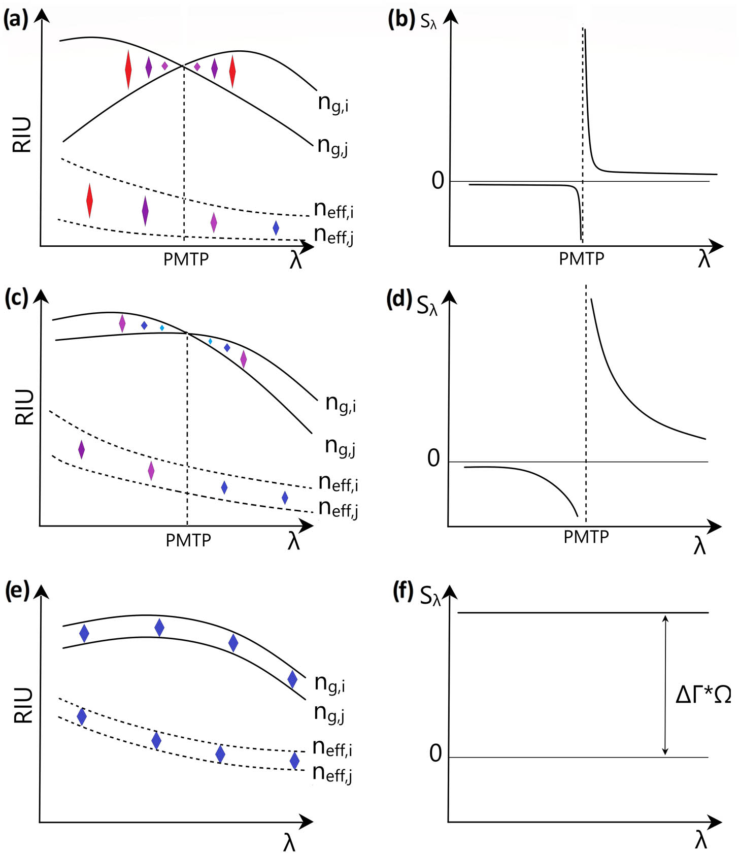
    Fig. 1. Illustration of spectral sensitivity optimization behavior. (a), (c), (e) Different propagation constant spectral profiles and (b), (d), (f) subsequent expected sensitivity behavior versus wavelength.
    Illustration of the implemented rib waveguide LPG structure with sinusoidally modulated width.
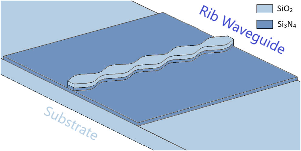
    Fig. 2. Illustration of the implemented rib waveguide LPG structure with sinusoidally modulated width.
    Simulated mode profiles for a rib LPWG: HE1 (top) and HE7 (bottom).
    Fig. 3. Simulated mode profiles for a rib LPWG: HE1 (top) and HE7 (bottom).
    LPG cross-sectional profile.
    Fig. 4. LPG cross-sectional profile.
    Coupling modes’ EI difference and waveguide sensitivity Γ difference versus slab etch depth with wslab=30 μm and wcore=1.65 μm at 1550 nm. Etch depth is set at e=35 nm and hslab=365 nm. Dashed lines: chosen etch depth and corresponding Δneff and ΔΓ.
    Fig. 5. Coupling modes’ EI difference and waveguide sensitivity Γ difference versus slab etch depth with wslab=30 μm and wcore=1.65 μm at 1550 nm. Etch depth is set at e=35  nm and hslab=365  nm. Dashed lines: chosen etch depth and corresponding Δneff and ΔΓ.
    Simulated effective and group indices of modes HE1 and HE7 showing similar dispersion with e=35 nm, wcore=1.65 μm, and wslab=30 μm.
    Fig. 6. Simulated effective and group indices of modes HE1 and HE7 showing similar dispersion with e=35  nm, wcore=1.65 μm, and wslab=30 μm.
    Coupling parameter and estimated full coupling length versus core width with e=35 nm and wslab=30 μm at 1550 nm. wcore is set at 1.65 μm. Dashed lines: chosen core width and corresponding coupling length Lopt and FWHM.
    Fig. 7. Coupling parameter and estimated full coupling length versus core width with e=35  nm and wslab=30 μm at 1550 nm. wcore is set at 1.65  μm. Dashed lines: chosen core width and corresponding coupling length Lopt and FWHM.
    Resonance spectra simulated with EME for different LPWG lengths with a period of 77.5 μm, e=35 nm, wslab=30 μm, and wcore=1.65 μm.
    Fig. 8. Resonance spectra simulated with EME for different LPWG lengths with a period of 77.5 μm, e=35  nm, wslab=30 μm, and wcore=1.65  μm.
    Layout of the designed photonic chip showing (a) strip–rib converter, (b) LPWG, and (c) grating coupler.
    Fig. 9. Layout of the designed photonic chip showing (a) strip–rib converter, (b) LPWG, and (c) grating coupler.
    Illustration of LPWG fabrication process.
    Fig. 10. Illustration of LPWG fabrication process.
    SEM pictures of photonic circuit components: (a) strip–rib converter; (b) grating coupler, (c) LPWG section, and (d) minor misalignment between strip and rib waveguides shown here at the beginning of the tapering region for the sake of clarity.
    Fig. 11. SEM pictures of photonic circuit components: (a) strip–rib converter; (b) grating coupler, (c) LPWG section, and (d) minor misalignment between strip and rib waveguides shown here at the beginning of the tapering region for the sake of clarity.
    Illustration of the experimental photonic characterization setup.
    Fig. 12. Illustration of the experimental photonic characterization setup.
    (a) Simulated and (b) experimentally measured normalized resonance spectra at surface RIs of 1.3388 and 1.34.
    Fig. 13. (a) Simulated and (b) experimentally measured normalized resonance spectra at surface RIs of 1.3388 and 1.34.
    Simulated and measured resonance wavelength of LPWGs obtained for different surface RIs.
    Fig. 14. Simulated and measured resonance wavelength of LPWGs obtained for different surface RIs.
    Experimental wavelength resonance pattern shifts with temperature of the LPWG.
    Fig. 15. Experimental wavelength resonance pattern shifts with temperature of the LPWG.
    Simulated and measured resonance wavelength variations versus temperature of the LPWG.
    Fig. 16. Simulated and measured resonance wavelength variations versus temperature of the LPWG.
    ReferencesMaterialStructure TypeLPG Length (μm)Measured Sensitivity (nm/RIU)FWHM (nm)Period (μm)
    [16]Silicon nitridePolymer waveguide coupling1000240–900510
    [13]BK-7 glassRib waveguide19152403180
    [12]Silicon nitrideStrip–slot waveguide coupling20001970715.1
    [14]SiliconAsymmetric strip waveguide1500507820–307.8
    Our workSilicon nitrideRib waveguide775011,5002577.5
    Table 1. Comparison with Other Fabricated LPWGs
    Clement Deleau, Han Cheng Seat, Olivier Bernal, Frederic Surre. High-sensitivity integrated SiN rib-waveguide long period grating refractometer[J]. Photonics Research, 2022, 10(2): 564
    Download Citation