Abstract
Er ions are implanted into the GaN thick films grown by hydride vapor phase epitaxy. The implantation energy is 200 keV and the implantation doses are , , , and , respectively. The effects of the implantation dose and annealing temperature on the GaN band-edge luminescence are investigated. The cathodoluminescence spectra from 82 to 323 K are measured for -implanted GaN annealed at 1100°C. Luminescence peaks at 356, 362, 376, 390, and 414 nm are observed on the 82 K cathodoluminescence spectrum. When the temperature is increased to 150 K, the intensities of the 356 and 414 nm peaks are nearly unchanged and the 362, 376, and 390 nm peaks disappear. The intensity ratio of 538 nm () and 559 nm () is increased with the increase in temperature. We try to shed light on the above interesting phenRare earth-doped GaN materials are promising for application in flat-panel displays, optical communication, solid-state lasers, ferromagnetic devices, etc.[1–4]. Red, green, and blue light was emitted from Eu, Er, and Tm-doped GaN materials, respectively[5–7]. For Er-doped GaN, 537 nm and 1.54 μm emissions were both observed[6,8]. Therefore, much attention was paid to the research of Er-doped GaN materials[9,10]. The preparation method of Er-doped GaN included ion implantation[11] and in situ doping[6]. High-concentration doping and selective-area doping can be finished by ion implantation. The drawbacks of ion implantation were that the crystal damage always exists in the GaN and needs to be recovered by high-temperature annealing.
Cathodoluminescence is a luminescence phenomenon where an electron beam interacts with materials. Because of the high energy of electron beams, cathodoluminescence spectroscopy is very suitable for the investigation of luminescence properties of wide bandgap semiconductors. There are few reports about the cathodoluminescence properties of Er-implanted GaN materials[12]. In this Letter, we systematically investigate the effects of implantation dose, annealing temperature, sample temperature on the cathodoluminescence properties of Er implanted GaN films.
GaN films with a 20 μm thickness were grown on the sapphire substrate by hydride vapor phase epitaxy. The Er ions with , , , and were implanted into the GaN films, respectively. The implantation energy was 200 keV and the implantation angle between the incoming beam and the crystal c axis was 10°. After implantation, the samples were annealed in the tube-type furnace with nitrogen gas with a flow rate of 0.6 sccm. The annealing temperatures were set as 800°C, 950°C, and 1100°C, respectively, and the annealing time was 1 h at each time. AlN samples were covered on the surface of the Er-implanted GaN samples for preventing the decomposition of the GaN surface.
Sign up for Chinese Optics Letters TOC. Get the latest issue of Chinese Optics Letters delivered right to you!Sign up now
Cathodoluminescence spectra were measured via a MonoCL3+ cathodoluminescence spectrometer installed on a Quanta400FEG scanning electron microscope. The slit width and the step of the spectrometer were set at 1 mm and 1 nm, respectively. The sample temperature was adjusted from 82 to 323 K.
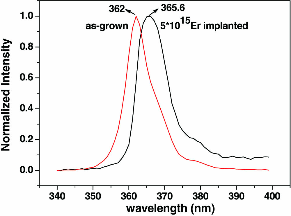
Figure 1 shows the spectra of virgin GaN and -implanted GaN. It was obvious that after implantation the GaN band-edge luminescence peak was shifted to a longer wavelength. The luminescence peaks of Er ions were not observed in these two samples.

Figure 1.Normalized room temperature cathodoluminescence spectra of virgin GaN and Er/cm2-implanted GaN.
Band-edge peaks and the FWHM of virgin GaN and Er-implanted GaN with different doses are listed in Table 1. Compared with the virgin GaN, the band-edge peak of Er-implanted GaN was redshifted 2–3.6 nm and the FWHM was increased by 0.5–1.3 nm. After Er implantation, most of the Er ions replaced the lattice sites of the Ga ions[13]. It is well known that the radius of Er ions is much bigger than that of Ga ions[14]. Therefore, the lattice constants of Er-implanted GaN became bigger after Er implantation and the bandgap became narrower. The redshift of band-edge luminescence was very obvious and reached 2 nm when the implantation dose was . With the increase in the implantation dose, the redshift value increased slowly. The FWHM of the band-edge peak became wider after Er implantation, which indicated that the crystal quality was decreased. Most of the Er ions replaced the lattice sites of the Ga ions. However, it is inevitable that a small quantity of Er ions and Ga ions entered into the interstitial sites because of the collision between Er ions and Ga ions in the process of implantation. Therefore, the periodicity of the crystal lattice became worse after Er implantation.
| Implantation dose of Er (atom/cm2) | Band-edge peak (nm) | FWHM (nm) |
|---|
| 0(virgin) | 362 | 8.5 |
| 1×10¹³ | 364 | 9.0 |
| 1×10¹⁴ | 365 | 9.3 |
| 1×10¹⁵ | 365 | 9.3 |
| 5×10¹⁵ | 365.6 | 9.8 |
Table 1. Position and FWHM of Cathodoluminescence Peaks of Virgin GaN and Er-Implanted GaN with Different Dosesa
It is well known that the rare earth ions in the implanted GaN were activated and showed the characteristic emission peaks after being annealed at a certain temperature[15]. The Er-implanted GaN was annealed and the annealing condition is described in the experiments section. For the implanted sample, the Er emission peaks were not observed after the 800°C or 950°C annealing. The strong Er emission peaks were observed after the 1100°C annealing, which indicated that the Er ions were activated adequately.
As shown in Table 2, the position and FWHM of the band-edge peaks of Er/cm2-implanted GaN before and after annealing are listed. After the 800°C or 950°C annealing, the peak position of the band-edge luminescence did not change, which indicated that most of the Er ions were still in the replacement position of the Ga ions and the bandgap did not change. On the other side, the FWHM decreased about 0.7 nm, which indicated that radiation damage was recovered to some extent. However, as shown in Fig. 2, after the 1100°C annealing the band-edge peak is redshifted from 365 to 367 nm, which indicates that some Er ions are left from the replacement position and combined with the surrounding defects[13]. The FWHM was decreased from 9.3 to 8.3 nm, which indicated that the radiation damage was partly recovered and the crystal quality became better.
| Annealing temperature (°C) | Band-edge peak (nm) | FWHM (nm) |
|---|
| unannealing | 365 | 9.3 |
| 800 | 365 | 8.6 |
| 950 | 365 | 8.6 |
| 1100 | 367 | 8.3 |
Table 2. Position and FWHM of the Band-Edge Peaks of 1×10¹⁵ Er/cm2-Implanted GaN Before and After Annealinga
Figure 2.Normalized room temperature cathodoluminescence spectra of -implanted GaN before and after annealing at 1100°C.
Figure 3 shows the normalized cathodoluminescence spectra of Er/cm2-implanted GaN after the 1100°C annealing. With the increase in the accelerating voltage, the absolute intensity of the band-edge luminescence and Er-ions luminescence both were increased. At the 5 kV accelerating voltage, the intensity of the Er luminescence at 537 and 558 nm was stronger than that of the band-edge luminescence. At 10 and 15 kV accelerating voltage, the intensity of the Er luminescence at 537 and 558 nm was weaker than that of the band-edge luminescence. At 5, 10, and 15 kV accelerating voltages, the intensity ratios of the 537 nm luminescence to band-edge luminescence were 13.755, 0.673, and 0.12, respectively. It was obvious that the change in the intensity ratio was more than 100 times that when the accelerating voltage was increased from 5 to 15 kV. The reason may be that GaN is a direct bandgap semiconductor and the intensity of the band-edge luminescence increases exponentially with the increase in accelerating voltage. However, under electron excitation, the Er-ion luminescence mechanism is collision excitation[1]. Therefore, the increase in the Er-ion luminescence intensity with the increase in the accelerating voltage is not as fast as the band-edge luminescence. On the other hand, the implantation depth of Er ions was only about 100 nm[11]. The penetration depth of electrons in GaN was increased from 90 to 900 nm when the accelerating voltage was increased from 5 to 15 kV[16]. Obviously, it is more favorable for band-edge luminescence.
Figure 3.Normalized room temperature cathodoluminescence spectra of -implanted GaN after 1100°C annealing, at different accelerating voltages of the scanning electron microscope.
The cathodoluminescence spectra of Er-implanted GaN annealed at 1100°C were measured at a 5 kV accelerating voltage. For -implanted GaN, Er luminescence was not observed. The cathodoluminescence spectra of , , and -implanted GaN are given in Fig. 4. With the increase in the Er dose, the intensity of the band-edge luminescence was decreased. When the Er dose was increased from to , the intensity of the band-edge luminescence was decreased about 15 times. The band-edge luminescence was not even observed in the cathodoluminescence spectra of the -implanted GaN, which indicated that the radiation damage was not easily recovered. When the Er dose was increased from to , the intensity of the Er luminescence was increased about 2 times. When the Er dose was increased from to , the intensity of the Er luminescence was decreased about 30%. The decrease of the Er luminescence may be caused by cross relaxation between Er ions[1]. We also calculated the Er concentration in the Er-implanted GaN. The implantation depth of Er was about 40 nm at 200 keV energy. It is well known that the number of Ga ions is in volume. Therefore, if the implantation dose was , , and , the concentration of Er was 0.056%, 0.56%, and 2.83%, respectively.
Figure 4.Room temperature cathodoluminescence spectra of Er-implanted GaN with different doses annealed at 1100°C. The accelerating voltage of the scanning electron microscope is 5 kV.
As shown in Figs. 5(a) and 5(b), the cathodoluminescence spectra of Er/cm2-implanted GaN annealed at 1100°C were measured at 82, 150, 223, 293, and 323 K, respectively. The peaks including 356, 362, 376, 390, and 414 nm were observed at the 82 K spectrum. The peak at 356 nm belonged to the free exciton peak[17]. The peaks at 362, 376, 390, and 414 nm were related to the Er implantation. The 362 nm peak may belong to the bound exciton peak of the surface defects[18]. After ion implantation, the surface roughness of the GaN was increased and the surface defects were produced[19]. The peak at 376 nm did not belong to the 2LO peak of free exaction, although the energy difference between the 376 and 356 nm peaks was about 185 meV which was nearly double that of one LO phonon with 92 meV energy. With the increase in temperature, the free exciton peak was shifted a to longer wavelength, but the peak at 376 nm was not moved. Furthermore, the peak at 376 nm was not observed in the cathodoluminescence spectra of the unimplanted GaN. Therefore, the peak at 376 nm most probably belonged to the donor-acceptor luminescence and the donor and acceptor both existed on the surface[18]. The peak at 390 nm belonged to the bound exciton luminescence, which was related to the point defects[18]. The peak at 414 nm belonged to deep energy level luminescence and needs to be investigated further. With the increase in temperature from 82 to 150 K, the free exciton luminescence shifted from 356 to 357 nm, and the peaks at 362, 376, and 390 nm disappeared, which indicated that the bound exciton was related to the surface defects and the donor-acceptor pair on the surface, and the bound exciton was related to the point defects being disassembled. On the other hand, with the increase in temperature from 82 to 293 K, the intensity of the band-edge luminescence did not obviously decrease, which may be related to the decomposition of the exciton, and the produced free electron and hole contributed to the band-edge luminescence. The intensity of the peak at 414 nm was nearly unchanged with the increase in temperature, which indicated that this peak was related to the deep energy level. However, when the temperature was increased to 323 K, the intensity of the peak at 414 nm decreased about 50%, which indicated that the carriers trapped at the deep energy level partly jumped out.
Figure 5.Cathodoluminescence spectra of Er/cm2-implanted GaN annealed at 1100°C. The temperature is from 82 to 323 K and the accelerating voltage of the scanning electron microscope is 5 kV.
The Er ion luminescence peaks at 538 and 559 nm were observed at room temperature. However, the luminescence peak at 538 nm was not observed at 82, 100, and 120 K. When the temperature was increased to 150 K, the 538 nm peak was observed. At room temperature, the intensity of the 538 nm peak was even stronger than that of the 559 nm peak. There is a thermal coupling between the and energy states[20]. At low temperatures, the state is not thermally populated and no luminescence was observed at 538 nm. When the temperature was increased to 150 K, the state was thermally populated; therefore, the luminescence at 538 nm was observed. At the same time, the intensity of the 559 nm luminescence was decreased to some extent. On the other hand, when the temperature was increased to 323 K, the intensity of 538 and 559 nm luminescence was not obviously decreased.
In conclusion, compared with the unimplanted GaN, the band-edge luminescence of the Er-implanted GaN is redshifted. The effects of the accelerating voltage on the intensity ratio of the 537 nm luminescence to the band-edge luminescence are investigated. Cross relaxation of Er ions is observed in Er-implanted GaN with the increase in the Er ion dose. There is a thermal coupling between the and energy state of . When the measured temperature is increased to 323 K, the intensity of the 538 and 559 nm luminescence of the Er ions does not obviously decrease, which indicates that Er-implanted GaN is promising for applications to the high temperature devices.
References
[1] A. J. Steckl, J. C. Heikenfeld, D. S. Lee, M. J. Garter, Christopher C. Baker, Yongqiang Wang, Robert Jones. IEEE J. Sel. Top. Quantum Electron., 8, 749(2002).
[2] H. Huang, D. Yan, G. Wang, F. Xie, G. Yang, S. Xiao, X. Gu. Chin. Opt. Lett., 12, 092301(2014).
[3] J. S. Kang, J. A. Yoon, S. I. Yoo, J. W. Kim, B. M. Lee, H. H. Yu, C. B. Moon, W. Y. Kim. Chin. Opt. Lett., 13, 032301(2015).
[4] C. P. Chen, H. J. Li, Y. Zhang, C. B. Moon, W. Y. Kim, C. G. Jhun. Chin. Opt. Lett., 12, 022301(2014).
[5] H. Bang, S. Morishima, J. Sawahata, J. Seo, M. Takiguchi, M. Tsunemi, K. Akimoto, M. Nomura. Appl. Phys. Lett., 85, 227(2004).
[6] S. Q. Chen, B. Dierre, W. Lee, T. Sekiguchi, S. Tomita, H. Kudo, K. Akimoto. Appl. Phys. Lett., 96, 181901(2010).
[7] N. Nepal, J. M. Zavada, D. S. Lee, A. J. Steckl, A. Sedhain, J. Y. Lin, H. X. Jiang. Appl. Phys. Lett., 94, 111103(2009).
[8] Q. Wang, R. Hui, R. Dahal, J. Y. Lin, H. X. Jiang. Appl. Phys. Lett., 97, 241105(2010).
[9] D. K. George, M. D. Hawkins, M. Mclaren, H. X. Jiang, J. Y. Lin, J. M. Zavada, N. Q. Vinh. Appl. Phys. Lett., 107, 171105(2015).
[10] A. Tahtamouni, M. Stachowicz, J. Li, J. Y. Lin, H. X. Jiang. Appl. Phys. Lett., 106, 121106(2015).
[11] N. Sathish, A. P. Pathak, G. Devaraju, E. Trave, P. Mazzoldi, S. Dhamodaran, V. N. Kulkarni. Radiat. Eff. Defects Solids, 167, 512(2012).
[12] H. J. Lozykowski, W. M. Jadwisienczak, I. Brown. Appl. Phys. Lett., 74, 1129(1999).
[13] J. Rodrigues, S. M. Cira Mnda, N. F. Santos, A. J. Neves, E. Alves, K. Lorenz, T. Monteiro. Mater. Chem. Phys., 134, 716(2012).
[14] M. M. Mezdrogina, E. Y. Danilovskii, R. V. Kuz’min. Inorg. Mater., 47, 1450(2011).
[15] C. Ronning, E. P. Carlson, R. F. Davis. Phys. Rep., 351, 349(2001).
[16] M. Staniforth, J. Goldstein, D. E. Newbury, C. E. Lyman, P. Echlin, E. Lifshin, L. C. Sawyer, J. R. Michael, D. C. Joy. Scanning Electron Microscopy and X-Ray Microanalysis(2002).
[17] M. A. Reshchikov, H. Morkoc. J. Appl. Phys., 97, 061301(2005).
[18] M. A. Reshchikov, D. Huang, F. Yun, P. Visconti, L. He, H. Morkoc, J. Jasinski, Z. Liliental-Weber, R. J. Molnar, S. S. Park. J. Appl. Phys., 94, 5623(2003).
[19] P. Ruterana, B. Lacroix, K. Lorenz. J. Appl. Phys., 109, 013506(2011).
[20] U. Hommerich, J. T. Seo, C. R. Abernathy, A. J. Steckl, J. M. Zavada. Mater. Sci. Eng., B81, 116(2001).