• Journal of Semiconductors
  • Vol. 42, Issue 1, 014102 (2021)
Jiajuan Shi, Ya Lin, Tao Zeng, Zhongqiang Wang, Xiaoning Zhao, Haiyang Xu, and Yichun Liu
DOI: 10.1088/1674-4926/42/1/014102 Cite this Article
Jiajuan Shi, Ya Lin, Tao Zeng, Zhongqiang Wang, Xiaoning Zhao, Haiyang Xu, Yichun Liu. Voltage-dependent plasticity and image Boolean operations realized in a WO x-based memristive synapse[J]. Journal of Semiconductors, 2021, 42(1): 014102 Copy Citation Text show less

Abstract

The development of electronic devices that possess the functionality of biological synapses is a crucial step towards neuromorphic computing. In this work, we present a WOx-based memristive device that can emulate voltage-dependent synaptic plasticity. By adjusting the amplitude of the applied voltage, we were able to reproduce short-term plasticity (STP) and the transition from STP to long-term potentiation. The stimulation with high intensity induced long-term enhancement of conductance without any decay process, thus representing a permanent memory behavior. Moreover, the image Boolean operations (including intersection, subtraction, and union) were also demonstrated in the memristive synapse array based on the above voltage-dependent plasticity. The experimental achievements of this study provide a new insight into the successful mimicry of essential characteristics of synaptic behaviors.

1. Introduction

The neuromorphic computing system is attracting significant interest to simulate the human brain due to its high fault tolerance and excellent power efficiency[1, 2]. Fabrication of electronic synapses is considered to be a key step towards hardware implementation of artificial neuromorphic systems. In recent work, the emerging memristor has been highlighted as a promising candidate to emulate synapses, thanks to its variable conductance in analogy with the change of synapse weight[3-6]. Various synaptic functions have already been demonstrated within memristors, including synaptic plasticity[7, 8], learning behaviors[4], and spike-timing-dependent plasticity (STDP)[9-11]. Among them, synaptic plasticity, including short-term plasticity (STP) and long-term potentiation (LTP), is responsible for the brain’s learning and memory processes at the cellular level[12, 13]. STP indicates that the enhanced synaptic weight is a transient process that lasts for only tens or hundreds of milliseconds. The permanent enhancement of synaptic weight (LTP) can only be observed in the case of repeated stimuli. According to previous reports, the employing of distinguishing spike frequency is the key to obtain enhanced conductance memory level, which enabled the realization of STP-to-LTP transition and experience learning. For example, Kim et al. achieved STP and the transition from STP to LTP using a biopolymer memristor by controlling the input pulse interval[14]. In our previous work, we demonstrated experience-dependent plasticity based on spike frequency sensitivity in a WOx memristor, which allowed us to reproduce the Bienenstock–Cooper–Munro learning rule and rate-based orientation selectivity[15]. In terms of stimuli conditions, stimulus intensity is a principal element for the learning and memory process, as is stimulus frequency. Abraham et al. demonstrated that LTP can be induced by conditioning stimuli with high intensity in the hippocampus[16]. Recently, Yang et al. demonstrated STP to LTP through adjusting electrical bias amplitude in the tungsten-oxide transistor synapse, presenting a new working approach to control the transition from short-term memory to long-term memory[17, 18]. But this behavior has been seldom reproduced in two-terminal memristive devices. Owing to the diversity of biological functions, it is still necessary to accurately simulate synaptic behaviors and expand their applications by regulating the properties of memristive materials.

In this paper, we report voltage-dependent STP in an Au/WOx/Ti memristive device. The transition from STP to LTP was achieved by increasing the amplitude of the applied voltage, and the sustained high-intensity stimulation induced permanent enhancement of conductance without any decay process. Moreover, the image Boolean operations were also demonstrated in a memristive synapse array based on voltage-dependent plasticity.

2. Experimental section

2.1. Fabrication of the device

The fabrication process of the Au/WOx/Ti device was as follows: first, Ti bottom electrodes (BEs) were deposited on a SiO2/Si substrate (SiO2 thickness 300 nm) by magnetron sputtering at a pressure of 1 Pa; second, a WOx layer was deposited on the Ti BEs by magnetron sputtering using a metal W target at room temperature. The film was prepared using mixed argon and oxygen (at a ratio of 1 : 1) at a pressure of 1 Pa. Finally, Au top electrodes (TEs) were thermally evaporated on the surface of the WOx film.

2.2. Electrical measurements of the device

The current–voltage (IV) measurements were taken using a Keithley 2636A source meter, and pulse measurements were obtained using an arbitrary function generator (3390, Keithley) and a digital oscilloscope (Keysight DSOS404A). The positive direction of the bias voltage was defined such that the current flowed from the top to the bottom electrode. A cross-sectional image of the device was obtained using an SEM (Nova Nano SEM 450).

3. Results and discussion

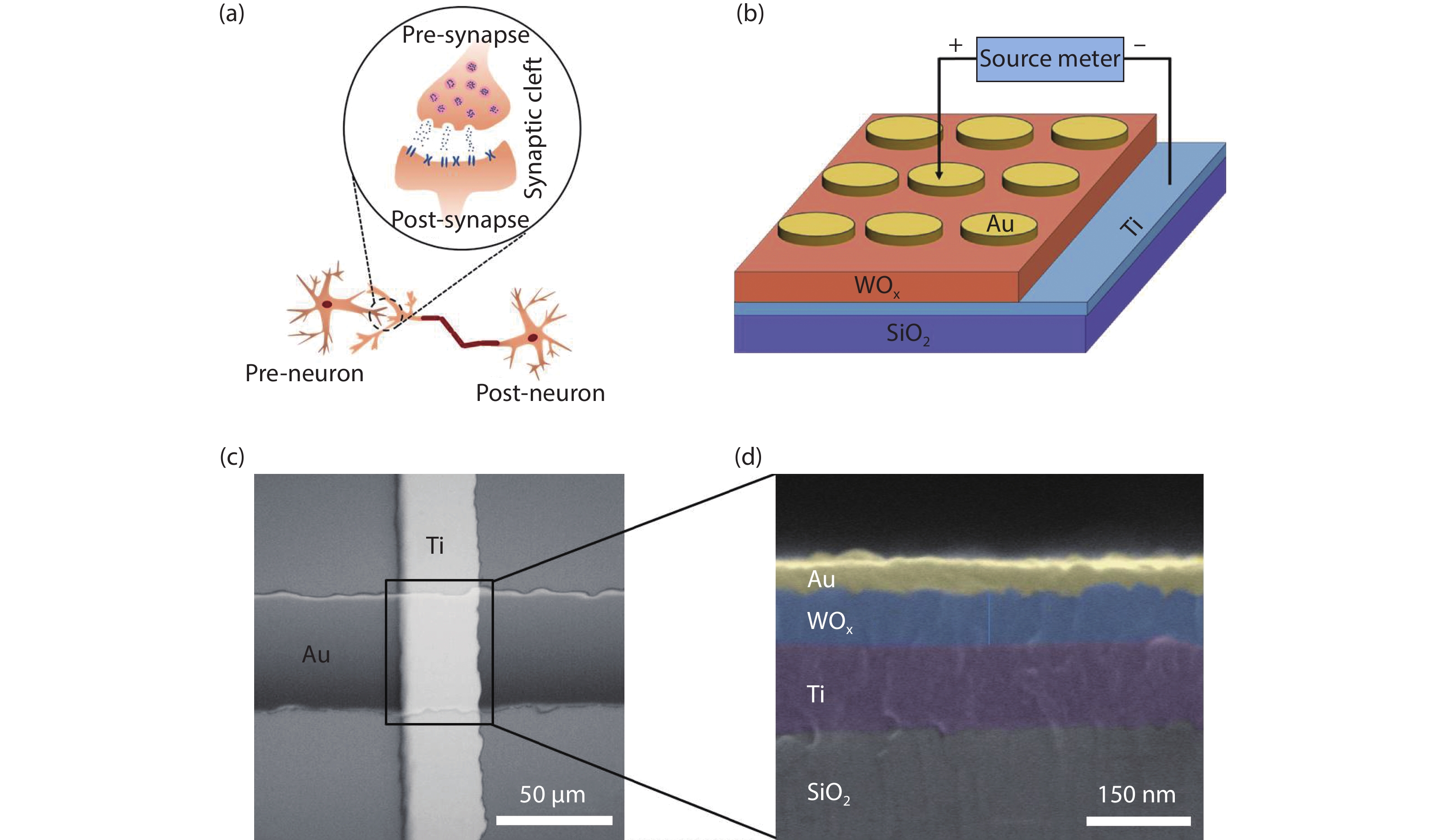
Fig. 1(a) shows a schematic of a synapse showing the pre-synapse, post-synapse, and synaptic cleft structure. The strength of a synapse can be dynamically tuned by external stimulation, which represents the neurochemical basis for learning and memory functions. In this study, the two-terminal memristor was designed to simulate a synapse (Fig. 1(b)). The electrical spike transferred from TEs to BEs, which corresponds to the transmission of biological signals from the pre-synaptic neuron to the post-synaptic neuron. Fig. 1(c) shows the as-prepared Au/WOx/Ti memristive device, which was prepared in crossbar arrays using the sputtering deposition technique. Our memristive device has a typical metal–insulation–metal (MIM) structure. As shown in the cross-sectional scanning electron microscope (SEM) image in Fig. 1(d), the 80-nm-thick WOx layer between the Au and Ti electrodes can be clearly seen, which demonstrates the two-terminal structure of this device.

(Color online) The structure and characterization of the Au/WOx/Ti memristive device. (a) Schematic illustration of the biological synapse connecting pre-synaptic and post-synaptic neurons. (b) Schematic illustration of the device, including Au top electrodes, WOx films and Ti bottom electrodes. (c) An overhead view of the device obtained by an optical microscope. (d) A cross-sectional SEM image of the device.

Figure 1.(Color online) The structure and characterization of the Au/WOx/Ti memristive device. (a) Schematic illustration of the biological synapse connecting pre-synaptic and post-synaptic neurons. (b) Schematic illustration of the device, including Au top electrodes, WOx films and Ti bottom electrodes. (c) An overhead view of the device obtained by an optical microscope. (d) A cross-sectional SEM image of the device.

The IV characteristics of the as-fabricated device were examined under a continuous voltage sweep, as shown in Figs. 2(a) and 2(b). The distinctive history-dependent memristive behavior was observed, whereby the device conductance could be continuously increased (decreased) with positive (negative) voltage sweeps. We found that the rectifying effect was observed during this process, which may be ascribed to the different Fermi levels between the Au electrode and WOx films. According to our previous study, the modulation of Au/WOx Schottky barrier height can account for analog resistive switching (A-RS) that occurs as a result of the migration and accumulation of oxygen ions[19, 20]. In neuromorphic systems, synaptic plasticity, which can be categorized into short-term plasticity (STP) and long-term plasticity, is an important characteristic for memory functions in the human brain[12]. One typical STP is paired-pulse facilitation (PPF), in which the excitatory postsynaptic current (EPSC) evoked by the second spike is larger than that of the first one. In this study, we investigated the influence of spike intensity on PPF behavior; Fig. 2(c) illustrates how PPF was measured in our synaptic device. Two continuous voltage spikes were applied to the synaptic device, and we defined the EPSC evoked by the first and second spike as P1 and P2, respectively. The PPF was calculated as follows:

(Color online) Demonstration of spike-intensity-dependent synaptic plasticity in a Au/WOx/Ti memristive device. (a, b) I–V characteristics of the device obtained under positive/negative bias; the voltage sweep range was 0 to 2 V (−2 V) then back to 0 V. (c) Schematic diagram of PPF measurement. (d) The variation of PPF according to relative spike timing.

Figure 2.(Color online) Demonstration of spike-intensity-dependent synaptic plasticity in a Au/WOx/Ti memristive device. (a, b) IV characteristics of the device obtained under positive/negative bias; the voltage sweep range was 0 to 2 V (−2 V) then back to 0 V. (c) Schematic diagram of PPF measurement. (d) The variation of PPF according to relative spike timing.

 (1)

As shown in Fig. 2(d), the PPF value depends on the time interval between two spikes (the amplitude varied from 0.4 to 2 V, the intervals varied from 1 to 200 ms and the duration was is fixed at 50 ms). The second spike enhanced the maximum current when it closely followed the first spike. Herein, the dependence of the PPF on the pulse interval (Δt) can be fitted by a double exponential function, which shows two-phase behavior:

 (2)

where t is the pulse interval time, C1 and C2 are the initial facilitation magnitudes of the respective phases, and τ1 and τ2 are the characteristic relaxation times of the respective phases. In the case of voltage amplitude with 2 V, τ1 and τ2 are 23 and 257 ms, respectively. The timescales of our memristive synapse are comparable to those of a biological synapse[12, 21]. More importantly, the spike amplitude greatly influenced PPF behavior. When the voltage was 0.2 V, the amplitude was too small to enhance the synaptic weight. On increasing the voltage, the higher spike amplitude led to a larger enhancement. In biology, the stimuli-intensity-dependent PPF effect is a result of the high residual Ca2+ concentration induced by the first spike and the overall Ca2+ level that is enhanced after the second spike. The synapse experiences a temporary increase in synaptic weight during this process.

STP can be transformed into long-term potentiation (LTP) through a rehearsal process, which was demonstrated in the memristor by using repeated high-frequency stimulation or increasing the number of stimulations[7, 14]. However, the influence of stimuli intensity on the transition from STP to LTP has seldom been reported. To demonstrate this transition, stimuli with different amplitudes were applied to the memristive synapse. All the pulse trains had a fixed frequency of 10 Hz and number of 30. Following this, weak stimuli (0.2 V, 10 Hz) were applied to monitor the memory state. As shown in Fig. 3(a), in the initial state, the device had a low conductance of about 0.6 μS due to the existence of a Schottky barrier between the Au and WOx layers. Weak stimuli with an amplitude of 1.5 V did not induce any enhancement of conductance after the stimuli ceased, which was indicative of STP behavior during this process. In contrast, strong stimuli with an amplitude of 3 V induced LTP in this memristive synapse, which retained high conductance even at 60 s after the stimulation ended. It is worth noting that a higher voltage can increase the conductance abruptly without any decay process (here, a 0.1 mA compliance current was set up to protect the device from hard breakdown). This high conductance state can maintain as long as 104 s, demonstrating the LTP characteristic in our device. The abrupt transition occurred because the conductive filaments linked the TE and BE. This behavior corresponds to the forming process, which is usually needed to form an initial conductive channel through the dielectric in the fresh resistive switching devices[22-24].

(Color online) The transition from STP to LTP by adjusting spike intensity. (a) The device received input stimuli with different features, including a spike train with an amplitude of 0.2 V, weak stimuli with an amplitude of 1.5 V, and strong stimuli with an amplitude of 3 V. (b) Memorization of the image “T” to demonstrate the transition from STM to LTM. Case 1: the conductance of the memristive array before stimulation, after 1.5-V stimulation, and after stimulation for 60 s; Case 2: the conductance of the memristive array before stimulation, after 3-V stimulation, and after stimulation for 60 s. The different color levels represent different magnitude conductance values.

Figure 3.(Color online) The transition from STP to LTP by adjusting spike intensity. (a) The device received input stimuli with different features, including a spike train with an amplitude of 0.2 V, weak stimuli with an amplitude of 1.5 V, and strong stimuli with an amplitude of 3 V. (b) Memorization of the image “T” to demonstrate the transition from STM to LTM. Case 1: the conductance of the memristive array before stimulation, after 1.5-V stimulation, and after stimulation for 60 s; Case 2: the conductance of the memristive array before stimulation, after 3-V stimulation, and after stimulation for 60 s. The different color levels represent different magnitude conductance values.

The mechanisms underlying the transition from STP to LTP are relevant to the short-term memory (STM) and long-term memory (LTM) models proposed by Atkinson and Shiffrin, in which the transition from STM to LTM occurs through a process of repetition[25]. In our work, the above behavior was also achieved by adjusting the voltage amplitude. As shown in Fig. 3(b), a 5 × 5 memristive synapse array, which was composed by 25 individual devices, was employed to memorize an image, the letter of “T”. The image “T” was inputted into the synapse array using 30 pulses with weak amplitude (1.5 V) and strong amplitude (3 V), respectively. The duration and interval time of the pulse were fixed at 50 ms. Before the stimulation, all the memristive synapses were randomly equipped with low conductance states. In case 1, the application of weak stimuli with an amplitude of 1.5 V temporarily increased the device conductance. The “T” image was stored in the memristive synapse array. However, this memorized image was totally forgotten after 60 s due to the STP effect. In case 2, strong stimuli with an amplitude of 3 V also increased the device conductance. However, in contrast to case 1, the “T” image could be stored after 60 s because the device was set to a high conductance state by the high voltage, which indicates that it achieved permanent memory.

It is interesting to note that the voltage-dependent plasticity allowed our devices to realize important logical operations. Boolean operations are key logical algorithms that are widely used in image processing[26, 27]. Boolean operations on two images X and Y can result in a new image, I, and the combination rule of two images can be classified as intersection (I = X ∩ Y), union (I = X ∪ Y), and subtraction (I = X − Y)[28, 29]:

 (3)

In this work, we successfully reproduced Boolean operations in our memristive synapse array. As shown in Fig. 4(a), 30 spike stimuli with an amplitude of 1.5 V (−1.5 V) and a duration of 50 ms were input from the pre-synapse (post-synapse) to implement the intersection operation, representing the input of image “X” (“Y”). Thus, the memristors in intersection part between “X” and “Y” undergo spike stimuli with an amplitude of 3 V. Fig. 4(b) shows the Boolean intersection operation: when training either the image “X” or “Y” in the memristive synapse array no image was obtained after 60 s due to the STP effect. When the “X” and “Y” images were input simultaneously, only the intersection part received stimuli with a high amplitude. The obtained image “V” could be memorized due to the LTP effect, which indicates the realization of the Boolean intersection operation.

(Color online) Demonstration of image Boolean intersection operation in the memristive synapse array. (a) The stimulation condition for inputting the images “X” and “Y”. (b) The conductance states of the devices under different inputting conditions.

Figure 4.(Color online) Demonstration of image Boolean intersection operation in the memristive synapse array. (a) The stimulation condition for inputting the images “X” and “Y”. (b) The conductance states of the devices under different inputting conditions.

Moreover, to reproduce Boolean subtraction and union operations, the amplitude of input stimuli was modified. Fig. 5(a) shows the input condition and the results of the subtraction operation. The spike stimuli with an amplitude of 3 V (1.5 V) were input from the pre-synapse (post-synapse); thus the intersection between “X” and “Y” received spike stimuli with an amplitude of 1.5 V. When the “X” and “Y” images were input simultaneously, only the part of “X” that was outside “Y” received 3 V stimuli and could be memorized after 60 s, which indicates that the Boolean subtraction operation was realized. Similarly, the spike stimuli with an amplitude of 3 V (−3 V) were input from the pre-synapse (post-synapse) to implement the union operation. As can be seen in Fig. 5(b), all the parts received high-intensity stimuli (above 3 V) and were memorized after 60 s, which indicates that the Boolean union operation was realized.

(Color online) Demonstration of the image. (a) Boolean subtraction and (b) Boolean union operations in the memristive synapse array.

Figure 5.(Color online) Demonstration of the image. (a) Boolean subtraction and (b) Boolean union operations in the memristive synapse array.

4. Conclusion

In summary, we demonstrated voltage-dependent synaptic plasticity in a WOx-based memristor, in which a higher voltage induced a larger enhancement of PPF. By increasing the spike amplitude, STP could be transformed to LTP, and sustained high-intensity stimulation induced permanent enhancement of conductance without any decay process. The voltage-dependent characteristic allows the memristor to reproduce image Boolean operations in the memristive synapse array. This work promotes the development of accurate and thorough simulation of synaptic behaviors that could have future neuromorphic applications.

Acknowledgements

This work was supported by the fund from Ministry of Science and Technology of China (Nos. 2018YFE0118300 and 2019YFB2205100), the NSFC Program (Nos. 11974072, 51701037, 51732003, 51872043, 51902048, 61774031, 61574031 and U19A2091), the “111” Project (No. B13013), the fund from Ministry of Education of China (No. 6141A02033414), and. The fund from China Postdoctoral Science Foundation (No. 2019M661185). The Fundamental Research Funds for the Central Universities (No. 2412019QD015), and the Fund from Jilin Province (JJKH20201163KJ).

References

[1] The future of electronics based on memristive systems. Nat Electron, 1, 22(2018).

[2] et alFully hardware-implemented memristor convolutional neural network. Nature, 577, 641(2020).

[3] et alMemristors with diffusive dynamics as synaptic emulators for neuromorphic computing. Nat Mater, 16, 101(2017).

[4] et alSynaptic learning and memory functions achieved using oxygen ion migration/diffusion in an amorphous InGaZnO memristor. Adv Funct Mater, 22, 2759(2012).

[5] et alMemristor with Ag-cluster-doped TiO2 films as artificial synapse for neuroinspired computing. Adv Funct Mater, 28, 1705320(2018).

[6] Memristive synapses for brain-inspired computing. Adv Mater Technol, 4, 1800544(2019).

[7] et alShort-term plasticity and long-term potentiation mimicked in single inorganic synapses. Nat Mater, 10, 591(2011).

[8] et alExperimental demonstration of a second-order memristor and its ability to biorealistically implement synaptic plasticity. Nano Lett, 15, 2203(2015).

[9] et alNanoscale memristor device as synapse in neuromorphic systems. Nano Lett, 10, 1297(2010).

[10] et alActivity-dependent synaptic plasticity of a chalcogenide electronic synapse for neuromorphic systems. Sci Rep, 4, 4906(2015).

[11] et alSTDP and STDP variations with memristors for spiking neuromorphic learning systems. Front Neurosci, 7, 2(2013).

[12] Short-term synaptic plasticity. Annu Rev Physiol, 64, 355(2002).

[13] Heterogeneity of synaptic plasticity at unitary CA3–CA1 and CA3–CA3 connections in rat hippocampal slice cultures. J Neurosci, 19, 10664(1999).

[14] Short-term plasticity and long-term potentiation in artificial biosynapses with diffusive dynamics. ACS Nano, 12, 1680(2018).

[15] et alToward a generalized Bienenstock-Cooper-Munro rule for spatiotemporal learning via triplet-STDP in memristive devices. Nat Commun, 11, 1510(2020).

[16] Single high strength afferent volleys can produce long-term potentiation in the hippocampus in vitro. Neurosci Lett, 70, 217(1986).

[17] et alArtificial synapses emulated by an electrolyte-gated tungsten-oxide transistor. Adv Mater, 30, 1801548(2018).

[18] et alDual-gated MoS2 transistors for synaptic and programmable logic functions. Adv Electron Mater, 6, 1901408(2020).

[19] et alTransferable and flexible artificial memristive synapse based on WOx Schottky junction on arbitrary substrates. Adv Electron Mater, 4, 1800373(2018).

[20] et alAnalog –digital hybrid memristive devices for image pattern recognition with tunable learning accuracy and speed. Small Methods, 3, 1900160(2019).

[21] Residual Ca2 + and short-term synaptic plasticity. Nature, 371, 603(1994).

[22] et alRoom-temperature developed flexible biomemristor with ultralow switching voltage for array learning. Nanoscale, 12, 9116(2020).

[23] Nanoionics-based resistive switching memories. Nanosci Technol, 158(2009).

[24] et alInsertion of nanoscale AgInSbTe Layer between the Ag electrode and the CH3NH3PbI3 electrolyte layer enabling enhanced multilevel memory. ACS Appl Nano Mater, 2, 307(2019).

[25] Human memory: A proposed system and its control processes. Psychol Learn Motiv, 2, 89(1968).

[26] Boolean operations on graphs. Math Scand, 20, 41(1967).

[27]

[28] Boolean operations of 2-manifolds through vertex neighborhood classification. ACM Trans Graph, 5, 1(1986).

[29] An algorithm reducing 3D Boolean operations to a 2D problem: concepts and results. Comput Aid Des, 28, 277(1996).

Jiajuan Shi, Ya Lin, Tao Zeng, Zhongqiang Wang, Xiaoning Zhao, Haiyang Xu, Yichun Liu. Voltage-dependent plasticity and image Boolean operations realized in a WO x-based memristive synapse[J]. Journal of Semiconductors, 2021, 42(1): 014102
Download Citation