• Acta Optica Sinica
  • Vol. 38, Issue 5, 0513001 (2018)
Yun Shen1, Tao Wang1, Yun Wang1, Xiaohua Deng、*, Juncheng Cao1, Zhiyong Tan1, Lin'er Zou1, and Guohong Dai1
Author Affiliations
  • 1 Department of Physics, Nanchang University, Nanchang, Jiangxi 330031, China
  • 1 Institute of Space Science and Technology, Nanchang University, Nanchang, Jiangxi 330031, China
  • 1 Key Laboratory of Terahertz Solid-State Technology, Chinese Academy of Sciences, Shanghai Institute of Microsystem and Information Technology, Chinese Academy of Sciences, Shanghai 200050, China
  • show less
    DOI: 10.3788/AOS201838.0513001 Cite this Article Set citation alerts
    Yun Shen, Tao Wang, Yun Wang, Xiaohua Deng, Juncheng Cao, Zhiyong Tan, Lin'er Zou, Guohong Dai. Broad-Band Polarization Characteristics on Transmission and Reflection of Metal Array Structures in Terahertz Region[J]. Acta Optica Sinica, 2018, 38(5): 0513001 Copy Citation Text show less
    Schematic of metal array structure
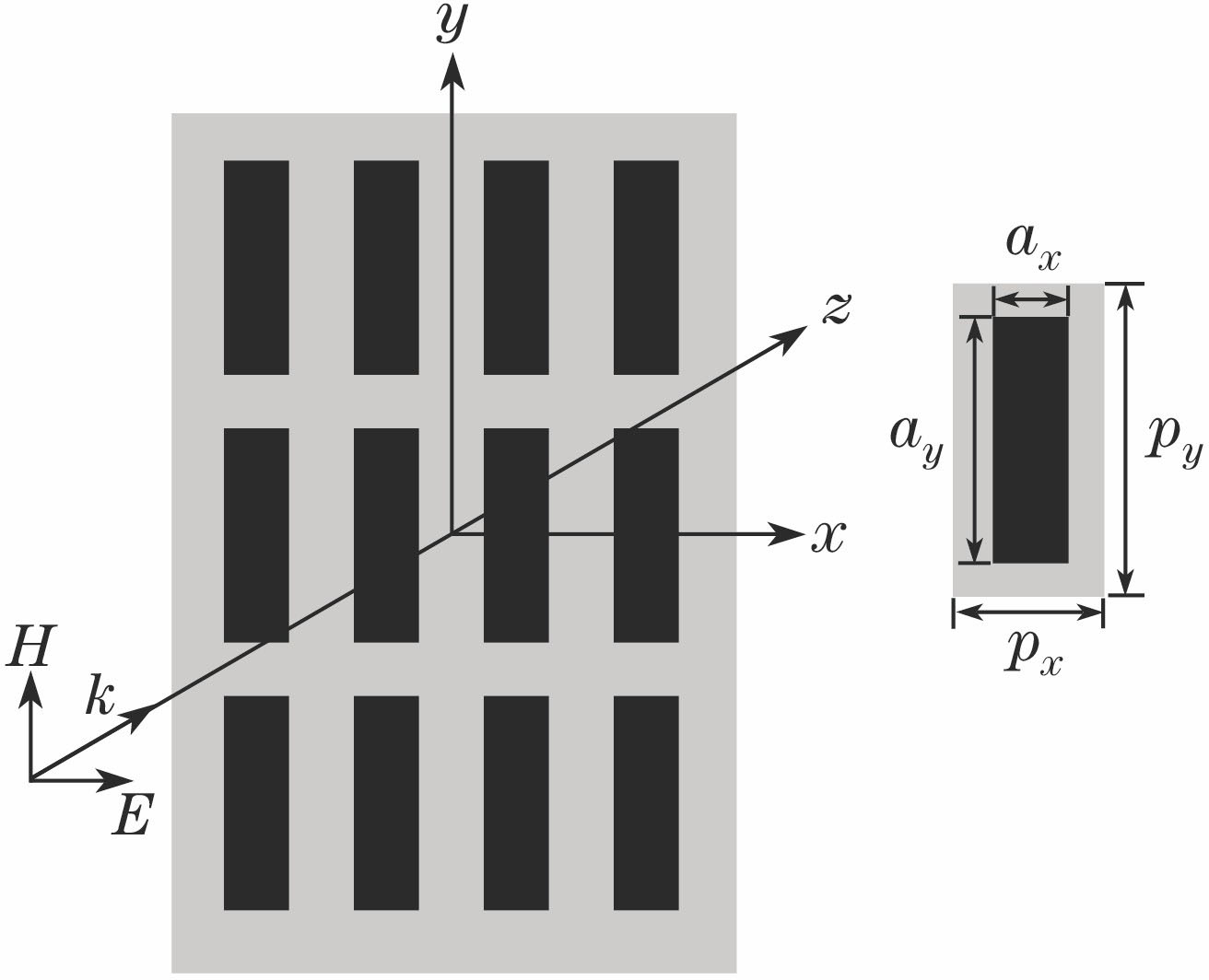
    Fig. 1. Schematic of metal array structure
    (a) Reflection spectrum lines and (b) transmission spectrum lines for TM/TE mode of metal array with and without Si substrate when the parameters of the array are Px=10 μm, ax=5 μm, Py=300 μm, and ay=250 μm
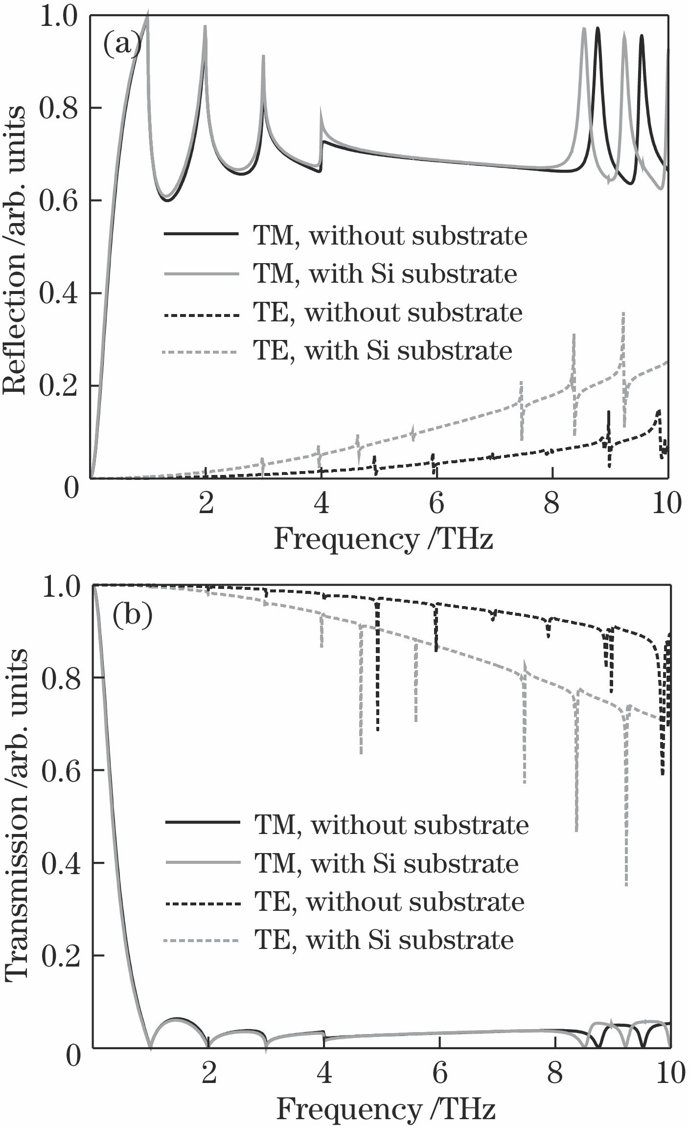
    Fig. 2. (a) Reflection spectrum lines and (b) transmission spectrum lines for TM/TE mode of metal array with and without Si substrate when the parameters of the array are Px=10 μm, ax=5 μm, Py=300 μm, and ay=250 μm
    (a) Reflection spectrum lines and (b) transmission spectrum lines for TM/TE mode of metal array with and without Si substrate when the parameters of the array are Px=20 μm, ax=10 μm, Py=300 μm, and ay=250 μm
    Fig. 3. (a) Reflection spectrum lines and (b) transmission spectrum lines for TM/TE mode of metal array with and without Si substrate when the parameters of the array are Px=20 μm, ax=10 μm, Py=300 μm, and ay=250 μm
    Optical micrograph and partial enlarged detail of the metal array with Px=10 μm and ax=5 μm
    Fig. 4. Optical micrograph and partial enlarged detail of the metal array with Px=10 μm and ax=5 μm
    Schematic of light path of measuring transmission spectrum lines and reflection spectrum lines
    Fig. 5. Schematic of light path of measuring transmission spectrum lines and reflection spectrum lines
    Measured (a) reflection spectrum lines and (b) transmission spectrum lines when the parameters of metal array are Px=10 μm, ax=5 μm, and the thickness of Si substrate is 500 μm
    Fig. 6. Measured (a) reflection spectrum lines and (b) transmission spectrum lines when the parameters of metal array are Px=10 μm, ax=5 μm, and the thickness of Si substrate is 500 μm
    Measured (a) reflection spectrum lines and (b) transmission spectrum lines when the parameters of metal array are Px=20 μm, ax=10 μm, and the thickness of Si substrate is 500 μm
    Fig. 7. Measured (a) reflection spectrum lines and (b) transmission spectrum lines when the parameters of metal array are Px=20 μm, ax=10 μm, and the thickness of Si substrate is 500 μm
    Yun Shen, Tao Wang, Yun Wang, Xiaohua Deng, Juncheng Cao, Zhiyong Tan, Lin'er Zou, Guohong Dai. Broad-Band Polarization Characteristics on Transmission and Reflection of Metal Array Structures in Terahertz Region[J]. Acta Optica Sinica, 2018, 38(5): 0513001
    Download Citation