
Chang Ge, Jing Li, Guohong Wang, Kang Su, Xingdong Lu. Size effect on optical performance of blue light-emitting diodes[J]. Journal of Semiconductors, 2019, 40(10): 102301
- Journal of Semiconductors
- Vol. 40, Issue 10, 102301 (2019)
Abstract
1. Introduction
Recently, micro-LED displays have been developing rapidly owing to their high dynamic range (HDR), high contrast ratio (CR), thin profile and low power consumption. Furthermore, with the growing interest in augmented reality (AR) and virtual reality (VR), the micro-LED displays with high pixels per inch (PPI) are strongly demanded, which means the ever-smaller LEDs are required. Generally, the size of micro-LEDs is smaller than 50 μm. Some groups have found that the micro-LEDs have higher nonradiative recombination, shorter response time[
In this study, a series of GaN-based LED chips with the same epilayer structure but different sizes were fabricated and the size effects of LEDs on the opto-electrical properties are further researched. In general, the micro-LED displays are driven by the constant current source with pulse width modulation. So we tested the external quantum efficiency, peak wavelength, full width at half maximum (FWHM) and other optical characteristics of these LEDs with different sizes driven by the direct current (DC) and PWM. It is found that these factors vary with the size of LEDs, which may be caused by stress release, surface recombination and thermal dissipation in different LEDs. The LED310 and the Agilent 33220A are used as DC and PWM power, respectively. The optical performance is tested by the integrating sphere and the HAAS-2000.
2. Experimental details
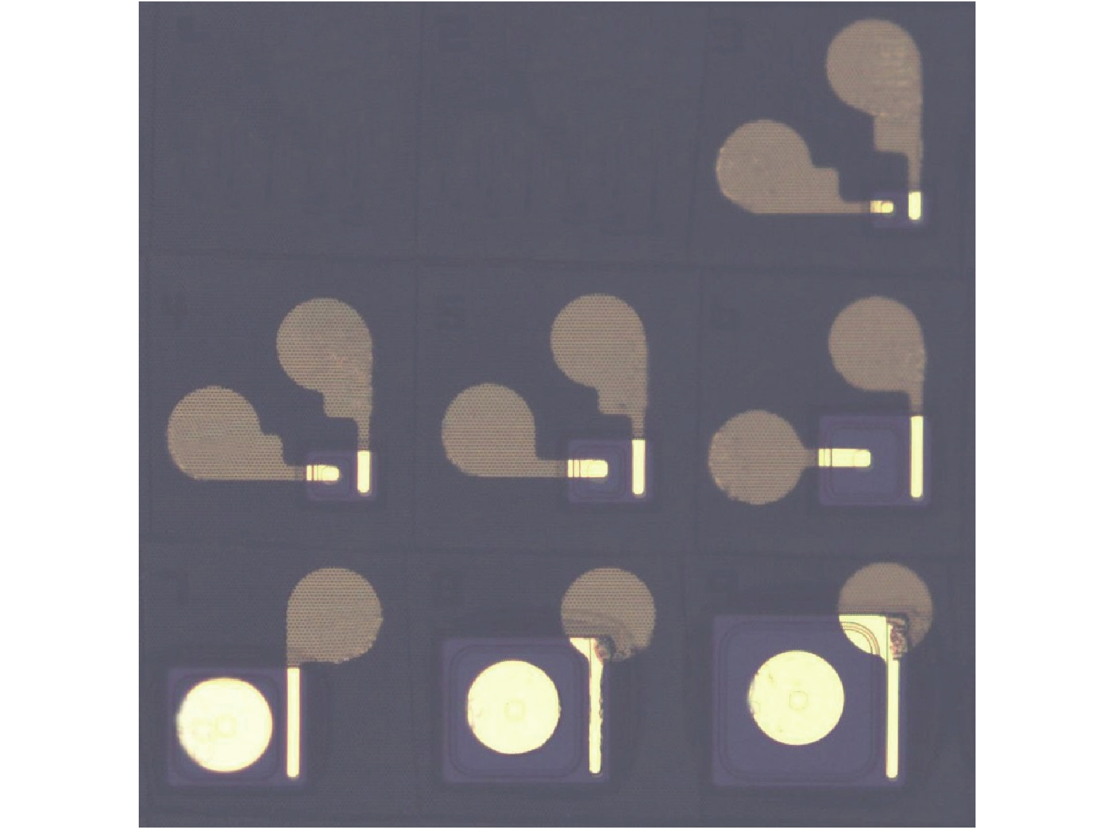
To eliminate machining errors, InGaN LED chips with seven different sizes were fabricated on the same epilayer structure for investigation. An optical micrograph of the fabricated LEDs with different dimensions is shown in Fig. 1. These chips all have a square active area with side length (D) ranging from 20 to 120 μm (20, 30, 40, 60, 80, 100, 120 μm respectively). Correspondingly, the size of the active area (S), the ratio of the perimeter (L) and the active area (S), the ratio of electrode area (LE) and the active area (S) are shown in Table 1. The main fabrication procedures of these LED chips with different sizes are as follow: cleaned the wafer, then formed the LEDs mesa structure by the photolithography and inductively coupled plasma (ICP) etching technique. Afterwards, these LEDs were isolated from each other using ICP etching technique. Thereafter, a silicon dioxide (SiO2) passivation layer was deposited by plasma-enhanced chemical vapor deposition (PECVD) and holes were formed at certain sites to support electrode connection by photolithography and buffered oxide etching (BOE). Finally, the metal layers were deposited by electron-beam evaporation and patterned by a lift-off procedure. The yellow areas in Fig. 1 are the electrodes.
![]()
Figure 1.(Color online) Optical micrograph of LEDs. The sizes of active area range from 20 to 120
3. Results and discussion
The J–V characteristics of micro-LEDs of varying sizes are plotted in Fig. 2. It is found that the LED of the smaller size exhibits the higher turn-on voltage and series resistance, which is ascribed to the larger dry-etching damage and the poor p-contact quality[
![]()
Figure 2.(Color online)
Fig. 3 shows the normalized external quantum efficiency (EQE) varying with current density of different LEDs. The EQE of seven different micro-LEDs shows a decreasing tendency with the increase in current density, which is called efficiency droop (ED).
![]()
Figure 3.(Color online) Normalized EQE vary with forward current density of micro-LEDs with different sizes.
From Eq. (1), the EQE is determined by two factors: the internal quantum efficiency (IQE) and the light extract efficiency (LEE). Dai et al.[
![]()
Figure 4.(Color online) Normalized EQE vary with chip size at 100, 300, and 500A/cm2.
Peak wavelength (λp) is plotted in Fig. 5(a) as a function of current density. At the same current density, the different peak wavelength is observed in these seven micro-LEDs even though they are grown on the same epilayer. It is found that the blue shift of the peak wavelength occurs with decrease of chip size, which attributes to the increasing bandgap caused by strain release[
![]()
Figure 5.(Color online) (a) Peak wavelength and (b) change of peak wavelength vary with forward current density of micro-LEDs with different sizes.
As shown in Fig. 6, full width at half maximum (FWHM) shows strong dependence on the chip size. The change of the FWHM is conspicuous for the small-size LED as the current increases, and it attributes to the junction temperature[
![]()
Figure 6.(Color online) Full width at half maximum (FWHM) varying with forward current of micro-LEDs with different sizes.
The pulse width modulation is adopted in the driving circuit of the LED displays generally. The PWM is a modulation technique for generating variable width pulses to represent the amplitude of an input analog signal or wave. Hence, the LED can be dimmed by the change of duty cycle. For LED displays, the stability of the domain wavelength (λd) is significant since humans can recognize color differences when the domain wavelength changes more than 0.1 nm. Therefore, the domain wavelengths of these seven different-size micro-LEDs are all tested under two different current density (100 and 500 A/cm2) driven by the PWM and the modulation frequency is 5 MHz. The effective current density is adjusted by the duty cycle from 90% to 10%. λd0 is identified as the domain wavelength when the duty cycle is 90%, and Δλd refers to the change of the domain wavelength which can be calculated by the equation Δλd = λd – λd0. The duty cycle dependence of Δλp for the different LEDs is plotted in Fig. 7. As shown in Fig. 7(a), the modulation current density is 500 A/cm2 and the λd of the broad-size LEDs is more stable, which is due to the redshift of wavelength caused by the junction temperature rising. However, when the modulation current density changes to 100 A/cm2 (Fig. 7(b)), the λd of the small-size LEDs is more stable. At the lower current density, the current injection in the small-size LEDs is much lower than the broad-size LEDs. Therefore, for small-size LEDs, the band-filling effect reduces and the domain wavelength changes slowly, which are more beneficial for displays.
![]()
Figure 7.(Color online) Current density dependence of Δ
4. Conclusion
In summary, we have investigated size effects on the optical performance of seven different-size LEDs. We find that smaller LEDs have great thermal dissipation and light extract efficiency. Besides, the surface recombination has an effect on EQE performance. At the low current density driven by PWM, the small-size LEDs have more stable wavelength because of the less carrier injection. That means micro-LED displays not only have higher PPI but have great wavelength stability.
Acknowledgments
This work was supported by National Key Research and Development Program of China (No. 2017YFB0404800).
References
[1] S X Jin, J Li, J Z Li et al. GaN microdisk light emitting diodes. Appl Phys Lett, 76, 631(2000).
[2] C W Jeon, H W Choi, P R Edwards et al. 64 × 64 matrix-addressable arrays of GaN-based micro-LEDs. Lasers & Electro-optics Society, Leos, the Meeting of the IEEE(2002).
[3] M Akhter. A LED micro-display with 90 × 90 pixels on a 80
[4] P Tian, J J D Mckendry, Z Gong et al. Characteristics and applications of micro-pixelated GaN-based light emitting diodes on Si substrates. J Appl Phys, 115, 033112(2014).
[5] Z Gong, E Gu, S R Jin et al. Efficient flip-chip InGaN micro-pixellated light-emitting diode arrays: promising candidates for micro-displays and colour conversion. J Phys D, 41, 094002(2008).
[6] C M Kang, D J Kong, J P Shim et al. Fabrication of a vertically-stacked passive-matrix micro-LED array structure for a dual color display. Opt Express, 25, 2489(2017).
[7] H W Choi, C W Jeon, M D Dawson et al. Fabrication and performance of parallel-addressed InGaN micro-LED arrays. IEEE Photonics Technol Lett, 15, 510(2003).
[8] Z Gong, S Jin, Y Chen et al. Size-dependent light output, spectral shift, and self-heating of 400 nm InGaN light-emitting diodes. J Appl Phys, 107, 013103(2010).
[9] Y B Tao, S Y Wang, Z Z Chen et al. Size effect on efficiency droop of blue light emitting diode. Physica Status Solidi C, 9, 616(2012).
[10] L Dai, N Zhang, J Y Lin et al. Comparison of optical transitions in InGaN quantum well structures and microdisks. J Appl Phys, 89, 4951(2001).
[11] F Demangeot, J Gleize, J Frandon et al. Optical investigation of micrometer and nanometer-size individual GaN pillars fabricated by reactive ion etching. J Appl Phys, 91, 6520(2002).
[12] S X Jin, J Shakya, J Y Lin et al. Size dependence of III-nitride microdisk light-emitting diode characteristics. Appl Phys Lett, 78, 3532(2001).
[13] H M Lu, G X Chen. Influence of polarization effect on optoelectronic properties of InGaN/GaN multiple quantum well. Chin J Lumin, 32, 266(2011).
[14] B Arnaudov, D S Domanevskii, S Evtimova et al. Band-filling effect on the light emission spectra of InGaN/GaN quantum wells with highly doped barriers. Microelectron J, 40, 346(2009).
[15] J H Ryou, P D Yoder, J Liu et al. Control of quantum-confined stark effect in ingan-based quantum wells. IEEE J Sel Top Quantum Electron, 15, 1080(2009).
[16] J Cho, C Sone, Y Park et al. Measuring the junction temperature of III-nitride light emitting diodes using electro-luminescence shift. Phys Status Solidi A, 202, 1869(2005).
[17] J Senawiratne, A Chatterjee, T Detchprohm et al. Junction temperature, spectral shift, and efficiency in GaInN-based blue and green light emitting diodes. Thin Solid Films, 518, 1732(2010).
[18]

Set citation alerts for the article
Please enter your email address
© Copyright 2018-2021 | Chinese Laser Press. All Rights Reserved 沪ICP备15018463号-20