
Tina Ebert, René Heber, Torsten Abel, Johannes Bieker, Gabriel Schaumann, Markus Roth. Targets with cone-shaped microstructures from various materials for enhanced high-intensity laser–matter interaction[J]. High Power Laser Science and Engineering, 2021, 9(2): 02000e24
- High Power Laser Science and Engineering
- Vol. 9, Issue 2, 02000e24 (2021)
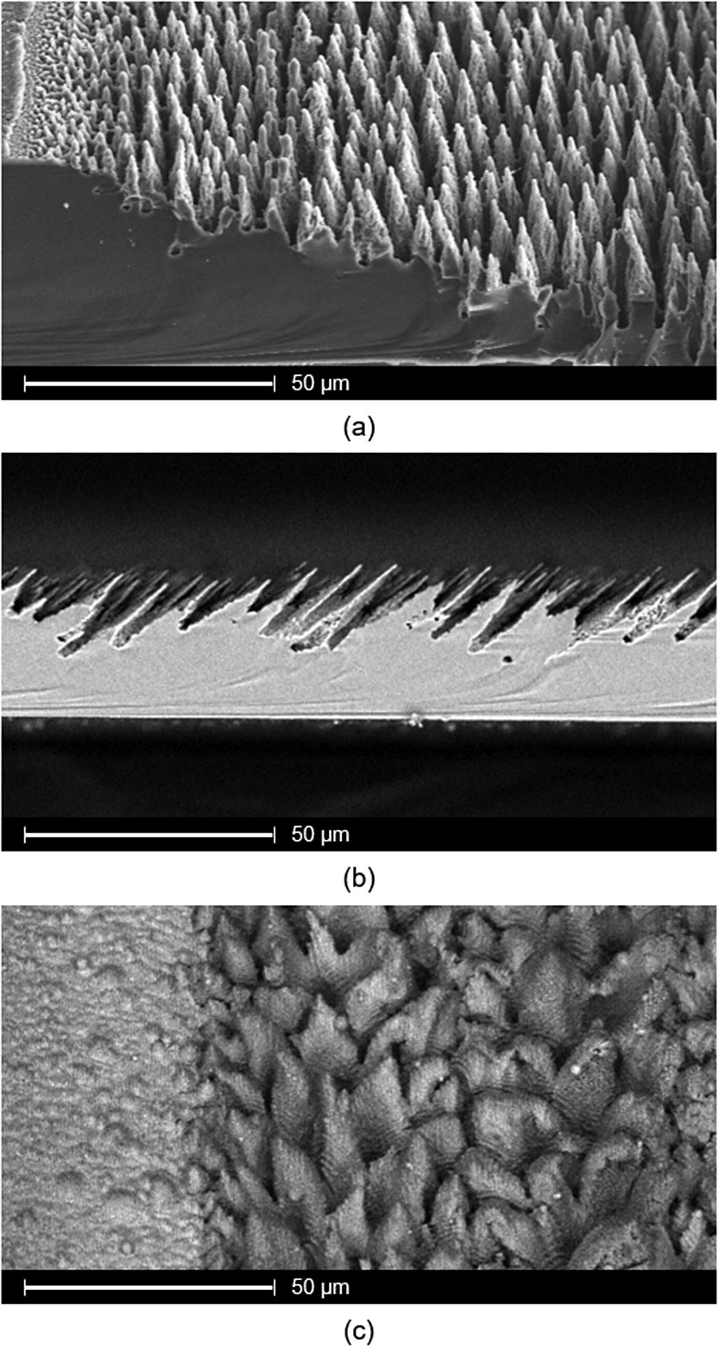
Fig. 1. SEM images of laser-induced microstructures. The top and middle images show cross sections of Si processed in 600 mbar SF6. For (a) the pulse number was increased from 0 to 1500 pulses from left to right at a fluence of approximately 8 kJ m . The sample is viewed at 30°. The slanted structures in (b) are created with a laser incidence angle of 45°, a fluence of approximately 9 kJ m
 and roughly 1000 pulses. This sample is viewed at 90°. The bottom image (c) shows Ti microstructures fabricated in 7 mbar vacuum with different laser fluences. Low fluences below the ablation threshold lead to ripples (left third) whereas higher fluences (up to 20 kJ m
 ) generate broad cones (two thirds on the right).
. The sample is viewed at 30°. The slanted structures in (b) are created with a laser incidence angle of 45°, a fluence of approximately 9 kJ m and roughly 1000 pulses. This sample is viewed at 90°. The bottom image (c) shows Ti microstructures fabricated in 7 mbar vacuum with different laser fluences. Low fluences below the ablation threshold lead to ripples (left third) whereas higher fluences (up to 20 kJ m) generate broad cones (two thirds on the right). 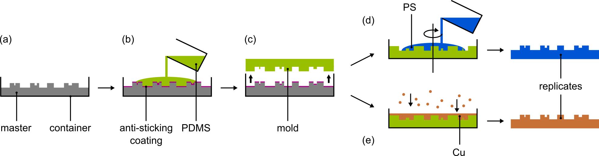
Fig. 2. Replication procedure. (a) The Si master is placed in a container and coated with an anti-sticking coating before (b) PDMS is poured onto it. (c) After solidification, the PDMS is removed and can then be used as a mould to either create (d) a PS replicate by spin coating or (e) a Cu replicate by thermal evaporation followed by electroplating.
Fig. 3. SEM images in top view of (a) Si needles fabricated in a SF6 environment and (b) a different section of the respective PDMS mould. The nanometre substructures of the master are clearly visible in the mould.
Fig. 4. SEM images viewed from the side with an approximate angle of 25° (left column) and from the top (right column). The top row shows a Si master, the middle row a PS replicate and the bottom row a Cu replicate. The lower magnification (2500×) of the side view illustrates the distribution and cone-shape of the structures whereas the higher magnification (7500×) of the images in top view shows the sub-micrometre features as well as the diameter of the structures.
Fig. 5. Layered target configurations as schematic (top row) and photo (bottom row). The PS foil (a) appears greenish on the rear side of the Si wafer with front surface microstructures. To create a defined laser-driven X-ray source, Cu microdots (b) are applied to the Si wafer before structuring the opposite side.

Set citation alerts for the article
Please enter your email address
© Copyright 2018-2021 | Chinese Laser Press. All Rights Reserved 沪ICP备15018463号-20