• Photonics Research
  • Vol. 11, Issue 8, 1382 (2023)
Yuechun Shi1、7、†, Shuiying Xiang2、†,*, Xingxing Guo2, Yahui Zhang2, Hongji Wang3, Dianzhuang Zheng1、2, Yuna Zhang2, Yanan Han2, Yong Zhao4, Xiaojun Zhu5, Xiangfei Chen3, Xun Li6, and Yue Hao2
Author Affiliations
  • 1Yongjiang Laboratory, Ningbo 315202, China
  • 2State Key Laboratory of Integrated Service Networks, State Key Discipline Laboratory of Wide Bandgap Semiconductor Technology, Xidian University, Xi’an 710071, China
  • 3Key Laboratory of Intelligent Optical Sensing and Manipulation, Ministry of Education, National Laboratory of Solid State Microstructures, College of Engineering and Applied Sciences, Institute of Optical Communication Engineering, Nanjing University, Nanjing 210023, China
  • 4School of Science, Jiangnan University, Wuxi 214122, China
  • 5School of Information Science and Technology, Nantong University, Nantong 226019, China
  • 6Department of Electrical and Computer Engineering, McMaster University, Hamilton, Ontario L8S 4K1, Canada
  • 7e-mail: yuechun-shi@ylab.ac.cn
  • show less
    DOI: 10.1364/PRJ.485941 Cite this Article Set citation alerts
    Yuechun Shi, Shuiying Xiang, Xingxing Guo, Yahui Zhang, Hongji Wang, Dianzhuang Zheng, Yuna Zhang, Yanan Han, Yong Zhao, Xiaojun Zhu, Xiangfei Chen, Xun Li, Yue Hao. Photonic integrated spiking neuron chip based on a self-pulsating DFB laser with a saturable absorber[J]. Photonics Research, 2023, 11(8): 1382 Copy Citation Text show less
    (a) Epitaxial wafer structure of the DFB-SA, (b) schematic of the fabricated DFB-SA chip, and (c) sample of the fabricated DFB-SA chip.
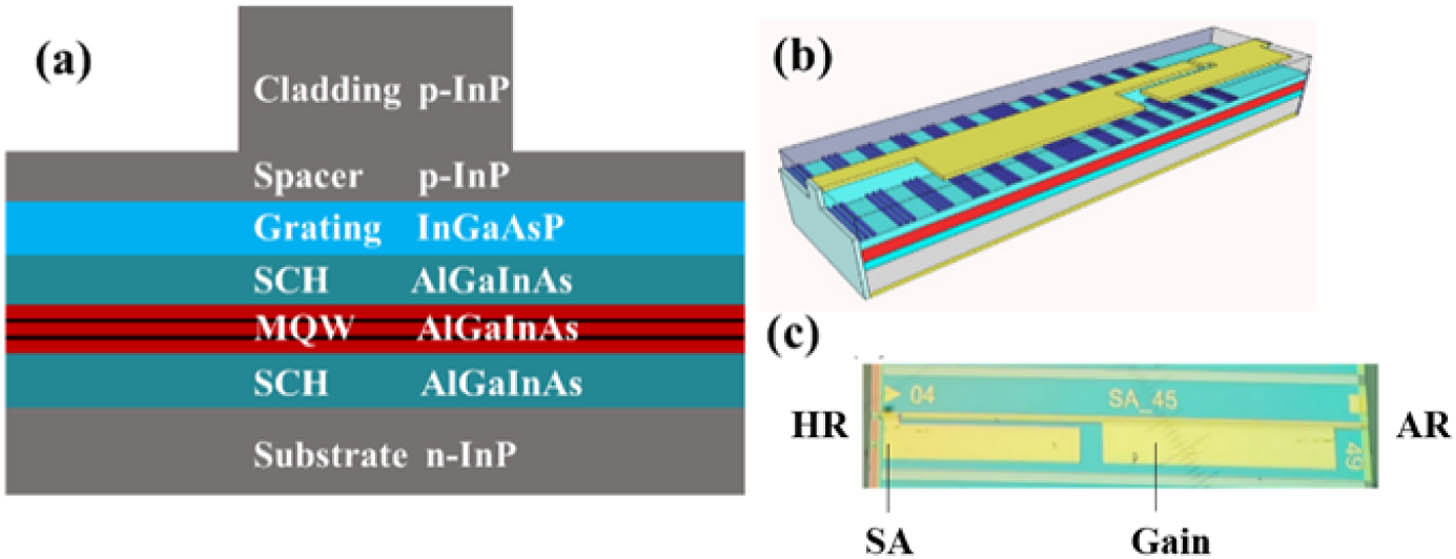
    Fig. 1. (a) Epitaxial wafer structure of the DFB-SA, (b) schematic of the fabricated DFB-SA chip, and (c) sample of the fabricated DFB-SA chip.
    (a) Experimental setup for a photonic spiking neuron based on the DFB-SA; (b) PI curves of the DFB-SA for VSA=0 V and VSA=−0.4 V; (c) optical spectra of the free-running DFB-SA for VSA=0 V, IG=99 mA and VSA=−0.4 V, IG=120 mA.
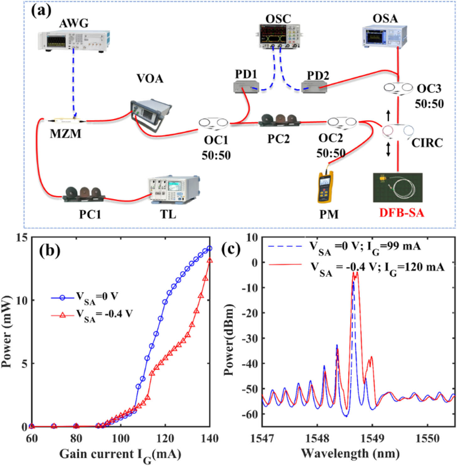
    Fig. 2. (a) Experimental setup for a photonic spiking neuron based on the DFB-SA; (b) PI curves of the DFB-SA for VSA=0  V and VSA=0.4V; (c) optical spectra of the free-running DFB-SA for VSA=0  V, IG=99  mA and VSA=0.4  V, IG=120  mA.
    (a1)–(a3) Time series of period spike outputs; (b1)–(b3) the corresponding power spectra of the DFB-SA for different gain currents with VSA=−0.4 V, IG=115 mA, IG=120 mA, and IG=130 mA.
    Fig. 3. (a1)–(a3) Time series of period spike outputs; (b1)–(b3) the corresponding power spectra of the DFB-SA for different gain currents with VSA=0.4  V, IG=115  mA, IG=120  mA, and IG=130  mA.
    Spike frequency as a function of the gain current for different cases of VSA.
    Fig. 4. Spike frequency as a function of the gain current for different cases of VSA.
    Excitability threshold property of DFB-SA subject to external perturbations. (a) The external stimulus; (b) the response output, the inset represents the enlargement of a single spike; (c) temporal maps plotting the response of the DFB-SA neuron to the arrival of 100 consecutive external stimuli with VSA=−0.4 V and IG=99.2 mA. The wavelength of the injected laser is 1548.61 nm.
    Fig. 5. Excitability threshold property of DFB-SA subject to external perturbations. (a) The external stimulus; (b) the response output, the inset represents the enlargement of a single spike; (c) temporal maps plotting the response of the DFB-SA neuron to the arrival of 100 consecutive external stimuli with VSA=0.4  V and IG=99.2  mA. The wavelength of the injected laser is 1548.61 nm.
    Temporal integration behavior of the DFB-SA spiking neuron: (a) the external stimulus with pulse pairs having different ISIs; (b) the response with VSA=−0.4 V and IG=94 mA. The ISI for seven pulse pairs is, respectively, 0.40 ns, 0.48 ns, 0.64 ns, 0.66 ns, 0.80 ns, 0.86 ns, and 1.0 ns.
    Fig. 6. Temporal integration behavior of the DFB-SA spiking neuron: (a) the external stimulus with pulse pairs having different ISIs; (b) the response with VSA=0.4  V and IG=94  mA. The ISI for seven pulse pairs is, respectively, 0.40 ns, 0.48 ns, 0.64 ns, 0.66 ns, 0.80 ns, 0.86 ns, and 1.0 ns.
    Refractory period behavior of the DFB-SA spiking neuron: (a) external stimulus with pulse pairs having different interspike interval; (b)–(f) the response under different conditions of the gain current. The gain current is, respectively, (b) 98.7 mA, (c) 104.4 mA, (d) 105.1 mA, (e) 111.0 mA, and (f) 112.1 mA. The ISI for seven pulse pairs is, respectively, 0.48 ns, 0.58 ns, 0.72 ns, 0.88 ns, 1.0 ns, 1.16 ns, and 1.24 ns.
    Fig. 7. Refractory period behavior of the DFB-SA spiking neuron: (a) external stimulus with pulse pairs having different interspike interval; (b)–(f) the response under different conditions of the gain current. The gain current is, respectively, (b) 98.7 mA, (c) 104.4 mA, (d) 105.1 mA, (e) 111.0 mA, and (f) 112.1 mA. The ISI for seven pulse pairs is, respectively, 0.48 ns, 0.58 ns, 0.72 ns, 0.88 ns, 1.0 ns, 1.16 ns, and 1.24 ns.
    Schematic of the DFB-SA subject to external optical injection.
    Fig. 8. Schematic of the DFB-SA subject to external optical injection.
    Numerical results of time series (left column) and power spectra (right column) of the self-pulsation output of the DFB-SA. (a) IG=45 mA, (b) IG=48 mA, and (c) IG=51 mA and ISA=0 mA.
    Fig. 9. Numerical results of time series (left column) and power spectra (right column) of the self-pulsation output of the DFB-SA. (a) IG=45  mA, (b) IG=48  mA, and (c) IG=51  mA and ISA=0  mA.
    Numerical results of the neuronlike response: (a) represents the stimuli; (b) represents the response with IG=41.7 mA and ISA=0 mA.
    Fig. 10. Numerical results of the neuronlike response: (a) represents the stimuli; (b) represents the response with IG=41.7  mA and ISA=0  mA.
    (a) The schematic of an ANN-to-SNN conversion using the photonics spiking neuron based on DFB-SA. (b) The activation function; the solid line is the curve of the measured data, and the dashed line is the corresponding polynomial fitting of the optical activation function. (c) The training and test accuracy for the MNIST dataset and (d) the confusion matrix of the inference task.
    Fig. 11. (a) The schematic of an ANN-to-SNN conversion using the photonics spiking neuron based on DFB-SA. (b) The activation function; the solid line is the curve of the measured data, and the dashed line is the corresponding polynomial fitting of the optical activation function. (c) The training and test accuracy for the MNIST dataset and (d) the confusion matrix of the inference task.
    SymbolDescriptionValue
    κGrating coupling coefficient1000  m1
    ΛGrating period242.0589 nm
    λBBragg wavelength1550 nm
    LLength of the laser cavity1500 μm
    LGLength of the gain section1480 μm
    LSALength of the SA section20 μm
    wWidth of the waveguide2 μm
    dThickness of the active layer60 nm
    λ0Reference wavelength1550 nm
    ALinear recombination coefficient1×108  s1
    BBimolecular recombination coefficient1×1016m3/s
    CAuger recombination coefficient3.5×1041  m3/s
    αsInternal loss5000  m1
    neff0Effective refractive index3.2
    ngGroup refractive index3.6
    NTTransparent carrier density1.5×1024  m3
    αmLinewidth enhancement factor1
    ΓConfinement factor0.08
    gNDifferential gain1.5×105  m1
    εGain suppression coefficient6×1023  m3
    γSpontaneous emission coefficient5×105
    Table 1. Basic Parameters Used in This Paper [33,34]
    Yuechun Shi, Shuiying Xiang, Xingxing Guo, Yahui Zhang, Hongji Wang, Dianzhuang Zheng, Yuna Zhang, Yanan Han, Yong Zhao, Xiaojun Zhu, Xiangfei Chen, Xun Li, Yue Hao. Photonic integrated spiking neuron chip based on a self-pulsating DFB laser with a saturable absorber[J]. Photonics Research, 2023, 11(8): 1382
    Download Citation