
Yuechun Shi, Shuiying Xiang, Xingxing Guo, Yahui Zhang, Hongji Wang, Dianzhuang Zheng, Yuna Zhang, Yanan Han, Yong Zhao, Xiaojun Zhu, Xiangfei Chen, Xun Li, Yue Hao. Photonic integrated spiking neuron chip based on a self-pulsating DFB laser with a saturable absorber[J]. Photonics Research, 2023, 11(8): 1382
- Photonics Research
- Vol. 11, Issue 8, 1382 (2023)
Abstract
1. INTRODUCTION
Artificial neural networks (ANNs) show great success in performing artificial intelligence tasks, such as image recognition, object detection, and object tracking. However, running ANN algorithms on a conventional von Neumann computer suffers from huge power consumption and large processing latency. The spiking neural network (SNN), which is usually regarded as the third generation of neural network, exhibits low power consumption and low latency when operating on neuromorphic hardware platforms. As a non von Neumann paradigm, neuromorphic computing has made significant progress in recent years [1–3]. Compared to the electronic counterparts, the photonic neuromorphic computing shows obvious advantages of high speed and energy efficiency [4–8], but it is still in its infancy.
Linear and nonlinear computations are the two fundamental functions of the photonic neuromorphic computing. The wavelength-division multiplexing architecture based on microring resonators [9,10], and the coherent architecture based on Mach–Zehnder interferometers [11–13], are the two mainstream approaches to implement the linear matrix-vector multiplication. Semiconductor lasers have become leading devices for the photonics nonlinear neuromorphic computing as their biologically plausible nonlinear neuronlike functions [14]. For instance, the spiking response has been demonstrated based on the polarization switching and injection locking effects in commercially available vertical-cavity surface-emitting lasers (VCSELs) [15–19]. In addition, the photonic SNN has been numerically studied for pattern recognition tasks based on the rate equation model of a VCSEL with a saturable absorber (SA) [20–22]. The refractory period property was observed experimentally in the micropillar lasers [23,24]. Photonic integrated circuits consisting of a two-section distributed feedback (DFB) laser and two photodetectors (PDs) were also proposed to emulate the spiking response [25,26]. In that approach, both sections of the DFB regions were positively biased, and the external optical stimulus signals were converted into the electronic signals via PDs and acted as driver currents of the two-section DFB laser. In addition, DFB lasers have also been demonstrated to work as graded-potential-signaling photonic neurons [27]. In our previous works, we designed and fabricated multi-longitudinal-mode photonic spiking neurons based on Fabry–Perot lasers with SAs [28,29]. Note that, in a hardware multilayer all-optical SNN, weighting devices and spiking neurons are coupled optically. Such multi-longitudinal-mode photonic spiking neurons can be compatible with the wide-bandwidth weighting devices but are not suitable for the narrow-bandwidth weighting devices. Therefore, it is still open to explore a novel single-longitudinal-mode photonic spiking neuron that is essential for the large-scale integrated photonic SNN with a narrow-bandwidth architecture.
In this paper, we proposed and experimentally demonstrated a photonic integrated spiking neuron based on a DFB laser with an intracavity SA (DFB-SA). The mechanism underlying the self-pulsation and neuronlike spiking response is revealed, and the operating conditions leading to the neuronlike dynamics are identified experimentally. The dependence of the self-pulsation frequency on the bias current in the gain region is revealed. A time-dependent coupled-wave equation model for the proposed DFB-SA is further developed. The rest of the paper is organized as follows. Section 2 describes the fabrication of the DFB-SA chip and the experimental setup for testing the photonic spiking neuron based on the DFB-SA chip. Section 3 presents the experimental results of the self-pulsation and neuronlike spiking response. The dependence of the self-pulsation frequency is revealed. The excitable spiking threshold, temporal integration, and refractory period results are all presented. The theoretical model and numerical results are presented in Sections 4 and 5. The rate encoding based on the controllable self-pulsation frequency has been applied successfully for an image recognition task of the handwritten digit dataset. By exploiting the ANN-to-SNN conversion, we achieved a testing accuracy of 92.2% with a single-layer fully connected network. Finally, the overall conclusion is summarized in Section 6.
Sign up for Photonics Research TOC. Get the latest issue of Photonics Research delivered right to you!Sign up now
2. DEVICE FABRICATION AND EXPERIMENTAL SETUP
As presented in Fig. 1(a), the epitaxial wafer structure consists of an -InP substrate, a buffer layer, two separate confinement heterostructure layers, strained multiple quantum wells with compressive strain quantum wells, tensile strain quantum barriers, an InGaAsP grating layer, and a -InP cladding layer. The grating is designed with a sampled grating. We shift the half period of the sampling structure in the middle of the DFB laser. This sampled grating structure can equivalently introduce a -phase shift (-EPS) as shown in Fig. 1(b) [30]. Here, the -EPS is realized by the reconstruction-equivalent-chirp (REC) technique. Compared to the conventional electron-beam lithography, the REC technique offers obvious advantages of low cost and precise wavelength control [31]. Anti-reflection (AR) and high-reflection (HR) coatings are applied to the two laser facets to improve the light emission power. Here, the SA region is designed near the HR side for an intracavity configuration as shown in Fig. 1(c), which is the micrograph picture of the fabricated DFB-SA chip. Then, the chip was further butterfly packaged without an isolator and was then tested for emulating a photonic spiking neuron.
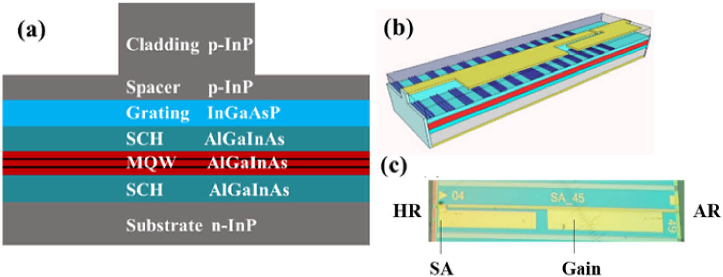
Figure 1.(a) Epitaxial wafer structure of the DFB-SA, (b) schematic of the fabricated DFB-SA chip, and (c) sample of the fabricated DFB-SA chip.
The experimental setup for testing the DFB-SA is shown in Fig. 2(a). A tunable laser generates a CW optical carrier. The CW light was injected into an intensity modulator, and an arbitrary wave generator (AWG, Tektronix AWG70001A) produced the defined external electronic stimulus. Two polarization controllers were employed before and after the intensity modulator to match the polarization state. Then, the modulated optical signal was injected into the DFB-SA without an isolator through a three-port optical circulator. The optical spectrum was measured by an optical spectrum analyzer (Advantest Q8384). Two PDs were employed to realize the optical–electronic conversion, and a real-time oscilloscope (OSC, Keysight DSOV334A, DSOZ592A) was utilized to measure the time series. The gain region of the DFB-SA is driven by a current source, and the SA region is reversely driven by a voltage source. The bias current in the gain region is denoted as the gain current , and the reversely biased voltage in the SA region is denoted as .
![]()
Figure 2.(a) Experimental setup for a photonic spiking neuron based on the DFB-SA; (b) PI curves of the DFB-SA for
The measured power-current curves for two representative cases of reversely biased voltages are depicted in Fig. 2(b). The threshold current of the DFB-SA is about for and is for . It is shown that, when a reversely biased voltage is applied, the threshold moves to a larger injection current, and the output power is decreased to some extent due to the absorption effect of the SA region. The optical spectrum of a free-running DFB-SA for and under the CW state is presented in Fig. 2(c). It can be seen that the peak wavelength is about 1548.66 nm. In addition, we can find that the optical spectrum for the case of and under self-pulsation is slightly broadened compared to the case of .
3. EXPERIMENTAL RESULTS
To begin with, we explore the self-pulsation behavior of the fabricated DFB-SA. Periodic excitable spike outputs can be observed when the bias current varies. Some representative periodic spike sequences are shown in Fig. 3. By fixing the reverse voltage of the SA as , we consider three cases of gain currents. The temporal output and the corresponding power spectra are displayed. It can be seen that for , the self-pulsation frequency is 0.703 GHz. For and , the frequencies are 0.938 GHz and 1.133 GHz, respectively. In addition, the pulse amplitude is also increased for a relatively large gain current.
![]()
Figure 3.(a1)–(a3) Time series of period spike outputs; (b1)–(b3) the corresponding power spectra of the DFB-SA for different gain currents with
To further reveal the self-pulsation condition, the spike frequency as a function of the gain current for different cases of is presented in Fig. 4. The laser thresholds are around 90 mA and 94 mA for the cases of and . When the gain current is biased above the laser threshold, the CW state is observed first, and then the self-pulsation state can be observed. We can find that, the range of the gain current that leads to the self-pulsation outputs is distinct for different cases of . When , for the gain current ranging from 115 to 132 mA, the self-pulsation output can be achieved, and the frequency is varied from 0.703 GHz to 1.25 GHz. For , the range of gain current leading to the self-pulsation output is from 123 mA to 152 mA, and the frequency is varied from 0.879 GHz to 1.78 GHz. For , in the range of the gain current from 141 mA to 174 mA, the DFB-SA operates in a periodic self-pulsation regime, and the frequency increases from 1.33 GHz to 2.25 GHz. Note, this self-pulsation property emulates the rate encoding of a biological neuron, and the spike frequency is much higher than the biological counterpart.
![]()
Figure 4.Spike frequency as a function of the gain current for different cases of
Next, we experimentally demonstrated the nonlinear neuronlike response of the DFB-SA. Here, the SA region is fixed at , and the gain current is biased below the self-pulsation threshold. The excitability threshold property is presented in Fig. 5. As can be seen in Figs. 5(a) and 5(b) for five input stimulus pulses with different intensities, four spikes are generated with almost the same intensity. The inset in Fig. 5(b) denotes the enlargement of a single spike. We can see that the full width at half maximum of the single spike is around 120 ps. The experimental color-coded temporal map plotting the superimposed time series of the responses corresponding to 100 consecutive arriving stimuli events is presented in Fig. 5(c). We can see that four distinguishable spikes can be observed in the two-dimensional map, indicating that the excitable behavior is reproducible in the experiment.
![]()
Figure 5.Excitability threshold property of DFB-SA subject to external perturbations. (a) The external stimulus; (b) the response output, the inset represents the enlargement of a single spike; (c) temporal maps plotting the response of the DFB-SA neuron to the arrival of 100 consecutive external stimuli with
In the following, we explore the temporal integration behavior of the fabricated DFB-SA. We designed several pulse pairs with different inter-spike-intervals (ISIs) as the external stimulus. The temporal time series of the stimulus and response are presented in Fig. 6. Here, the first single weak pulse and the last single strong pulse are designed as reference pulses. We consider that the single weak pulse is below the excitable threshold, whereas, the single strong pulse exceeds the excitable threshold. It can be seen that, the single weak stimulus pulse cannot trigger a spike response, whereas, the last strong pulse can produce a spike response. In addition, when the ISI is not greater than 0.66 ns, four spikes are generated for the first four closely spaced pulse pairs with relatively small ISIs. For the last three pulse pairs with large ISIs, the two stimulus pulses cannot temporally integrated and cannot exceed the excitable threshold. Thus, the DFB-SA emulates the leaky integrate-and-fire (LIF) neuron [32].
![]()
Figure 6.Temporal integration behavior of the DFB-SA spiking neuron: (a) the external stimulus with pulse pairs having different ISIs; (b) the response with
To emulate the refractory property, we also designed several pulse pairs as the external stimuli. Here, we also introduce a single pulse as the reference pulse. The stimulus signal is presented in Fig. 7(a). The stimuli intensity is chosen to ensure that the first single pulse can trigger a spike response. As presented in Figs. 7(b)–7(f), different gain currents lead to different refractory periods. In Fig. 7(b), for , only the single spike is produced for each pulse pair. For , two spikes can be generated for the last pulse pair with ISI of 1.24 ns. With the increase of the gain current, two spikes can be generated for a greater number of pulse pairs. Namely, the refractory period is decreased with the increase of the gain current. In the experiment, we find that the bias current of the gain region, the reverse voltage of the SA region, as well as the injection optical power can all affect the refractory period, which is associated with the carrier recovery process [28]. In practice, the spiking processing speed is limited by the refractory period.
![]()
Figure 7.Refractory period behavior of the DFB-SA spiking neuron: (a) external stimulus with pulse pairs having different interspike interval; (b)–(f) the response under different conditions of the gain current. The gain current is, respectively, (b) 98.7 mA, (c) 104.4 mA, (d) 105.1 mA, (e) 111.0 mA, and (f) 112.1 mA. The ISI for seven pulse pairs is, respectively, 0.48 ns, 0.58 ns, 0.72 ns, 0.88 ns, 1.0 ns, 1.16 ns, and 1.24 ns.
In our experiments, the fabricated DFB-SA chip can emulate the rate encoding mechanism and can also emulate the neuronlike response of an LIF neuron. Thus, the DFB-SA chip can be used as a fundamental building block of photonic SNN.
4. THEORETICAL MODEL
In a DFB laser, due to the distributed feedback provided by the Bragg grating, the carrier density and optical field are nonuniform along the laser cavity. Here, we adopt the well-known time-dependent coupled-wave equations to verify the experimental findings. We modify the model to introduce the gain region, SA region, as well as the external optical injection term. A schematic of the DFB-SA subject to external optical injection is presented in Fig. 8.
![]()
Figure 8.Schematic of the DFB-SA subject to external optical injection.
The rate equations for the carrier density in the gain region and SA region , and the coupled-mode equations for the slowly varying envelopes of the forward traveling wave and backward traveling wave can be expressed as follows [33–35]:
Specifically, in Eq. (4), the first term on the right-hand side represents the effect of reverse voltage of the SA region. Note that, there is no direct and simple method to introduce the reverse voltage in the rate equation. Thus, we introduce a reverse bias current to be equivalent to the effect of reverse voltage for simplicity. The second term denotes the depletion of carrier due to the carrier lifetime, and the third term accounts for the increase in carrier due to the absorption.
Here, can be expressed as
The material absorption coefficient of the SA region can be phenomenologically introduced as
The variables and denote the detuning factor and photon density, which are given, respectively, by [33,34]
The effective refractive index is given by
The noise terms are assumed to be a Gaussian distributed random process that satisfies
The boundary conditions including the facet reflections and the external injection can be expressed as [36]
The basic parameters are given in Table 1. With these parameters, we numerically solve the time-domain traveling wave model with the split-step finite difference method. The whole laser cavity is split to several tens of subsections with a length of , where denotes the time step. Basic Parameters Used in This Paper [Symbol Description Value Grating coupling coefficient Grating period 242.0589 nm Bragg wavelength 1550 nm Length of the laser cavity 1500 μm Length of the gain section 1480 μm Length of the SA section 20 μm Width of the waveguide 2 μm Thickness of the active layer 60 nm Reference wavelength 1550 nm Linear recombination coefficient Bimolecular recombination coefficient Auger recombination coefficient Internal loss Effective refractive index 3.2 Group refractive index 3.6 Transparent carrier density Linewidth enhancement factor 1 Confinement factor 0.08 Differential gain Gain suppression coefficient Spontaneous emission coefficient
5. NUMERICAL RESULTS
Based on the time-dependent coupled-wave model, we further numerically verified the experimental findings. Here, we consider . As shown in Fig. 9 with the increase of the gain current, the self-pulsation frequency is increased.
![]()
Figure 9.Numerical results of time series (left column) and power spectra (right column) of the self-pulsation output of the DFB-SA. (a)
Then, we consider the neuronlike response of the DFB-SA subject to optical pulse injection. As displayed in Fig. 10, the absolute refractory period, relative refractory period, temporal integration, and spike threshold properties can all be observed numerically. These numerical results agree well with the experimental findings. Note, due to the complicated parameters of the DFB-SA, such as the grating coupling coefficient, internal loss, and the HR facet random phase, the bias currents in the simulation are a little different from the experiments, but the simulated self-pulsation and neuronlike response can reveal the dynamics process of a DFB-SA. Thus, this time-dependent coupled-wave model provides valuable guidelines for the design and optimization of the DFB-SA chip, which is helpful for the hardware-algorithm codesign for photonic SNNs.
![]()
Figure 10.Numerical results of the neuronlike response: (a) represents the stimuli; (b) represents the response with
At last, we adopt the experimentally measured dependence of the spike frequency on the gain current as the spiking activation function. For the Modified National Institute of Standards and Technology (MNIST) handwritten digit classification task [37], the input image of a handwritten digit is . A simple single-layer fully connected neural network is considered. The input layer contains 784 neurons, and the output layer contains 10 neurons as presented in Fig. 11(a). In ANN training, the fitted curve of the dependence of the spike frequency on the gain current as shown in Fig. 11(b) is used as the activation function. The ANN is trained with the backpropagation method. Note, we only consider the non-negative weight in training, which can also be regarded as nonlinear activation before summation [38]. The inference process is accomplished with the ANN-to-SNN conversion [39]. The output class is encoded into the self-pulsation frequency. Similar to the output decision of ANN, the output neuron with the highest frequency is considered as the output class. The training accuracy and the testing accuracy are presented in Fig. 11(c). The confusion matrix is presented in Fig. 11(d). Numbers on the diagonal line represent the recognition accuracy. The accuracy reaches 92.2%, which bridges the gap between the continuous-valued ANN and spike-based neuromorphic network. Note, if hidden layers or convolution layers are introduced, the accuracy can be further increased.
![]()
Figure 11.(a) The schematic of an ANN-to-SNN conversion using the photonics spiking neuron based on DFB-SA. (b) The activation function; the solid line is the curve of the measured data, and the dashed line is the corresponding polynomial fitting of the optical activation function. (c) The training and test accuracy for the MNIST dataset and (d) the confusion matrix of the inference task.
6. CONCLUSIONS
We proposed and experimentally demonstrated the rate encoding mechanism as well as the neuronlike spiking response in a fabricated DFB-SA chip. The experimental results showed that the self-pulsation frequency is increased with the increase of the bias current in the gain region. In addition, the neuronlike nonlinear computation including the excitable spiking threshold, temporal integration, and refractory period were successfully observed in the experiment. We also verified the experimental findings with the time-dependent coupled-wave model. We further applied the experimentally measured dependence of the spike frequency on the gain current as the optical spiking activation function, and realized the pattern classification task. By adopting the ANN-to-SNN conversion, we achieved the test accuracy of 92.2% with the single-layer fully connected network. Note that, the DFB-SA can be designed with a multichannel and can be integrated with other photonic devices [30], which paved the way for realizing large-scale photonic spiking neural chips. As a future attempt, it was also interesting to design this DFB-SA chip on silicon [40] to be better compatible with the silicon photonics synaptic network, thus, realizing full-function photonic spiking neuron network chip.
References
[32] E. M. Izhikevich. Dynamical Systems in Neuroscience(2007).
[35] X. Li. Optoelectronic Devices: Design, Modeling, and Simulation(2009).
[37] http://yann.lecun.com/exdb/mnist/. http://yann.lecun.com/exdb/mnist/
[40] N.-P. Diamantopoulos, S. Yamaoka, T. Fujii, H. Nishi, T. Segawa, S. Matsuo. Ultrafast spiking membrane III-V laser neuron on Si. European Conference on Optical Communication (ECOC), 1-4(2022).

Set citation alerts for the article
Please enter your email address
© Copyright 2018-2021 | Chinese Laser Press. All Rights Reserved 沪ICP备15018463号-20