Beijing Key Laboratory of Millimeter Wave and Terahertz Technology, School of Information and Electrics, Beijing Institute of Technology, Beijing 100081, China
A simple and effective design method for high cut-off frequency Schottky barrier diode is proposed and implemented. The cut-off frequency of the processed Schottky barrier diode is about 800 GHz, which can reach about 1 THz with the optimized parameters through the test results and simulation data in SMIC 180 nm process. The integrated detector including antennas, matching circuit and Schottky barrier diode is completed, whose tested responsivity could achieve 130 V/W and noise equivalent power is estimated to be 400 pW/ at 220 GHz. The imaging experiment of invisible liquid surface in ceramic bottles has been completed and good results have been achieved.
Lately,focus on terahertz(THz)technology has been growing rapidly owing to its great potential in the fields of imaging,medical,communication,astronomy,etc.[1-2]. A number of studies have been reported on THz imaging system,which is closer than spectroscopy to being commercialized in the near future[3]. complementary metal oxide semiconductor(CMOS)technology attracts high attention in THz imaging filed with its low cost and high integration,which meets the needs of THz large-scale imaging array[4].
Two major THz detectors in the CMOS field have been extensively studied,filed-effect transistor(FET)detectors based on plasma-wave detection theory and Schottky barrier diode(SBD)detector based on square law detector theory[5-6]. Compared with FET detectors,SBD detectors have obvious advantages in responsivity,which is extremely important for THz imaging owing to the inherent high spatial loss of THz wave[7-8]. Since V.Milanovic and Sankraran successively realize Schottky contact in CMOS process by metallizing the contact on the n-well and contacting the metal silicide with the substrate,many related studies have been done on CMOS SBD[9]. Nevertheless,there is no SBD applicable to THz band in the existing standard CMOS library,which is a hot point and difficulty in the THz study field.
The CMOS technology-based THz detectors with different detection mechanisms including plasma modes and Schottky barrier diodes have very high requirements for cut-off frequency. The cut-off frequency of SBD is closely related to the minimum size that CMOS technology can achieve. Many high cut-off frequency detectors come to the fore with the progress of technology. For example,a 0.86-THz 4 × 4 array CMOS technology-based SBD imager is reported with raster scan measurement[10-11],and a 1 × 240 array compound InGaAs SBD imager is demonstrated as a real-time 1-D line scanner[12].
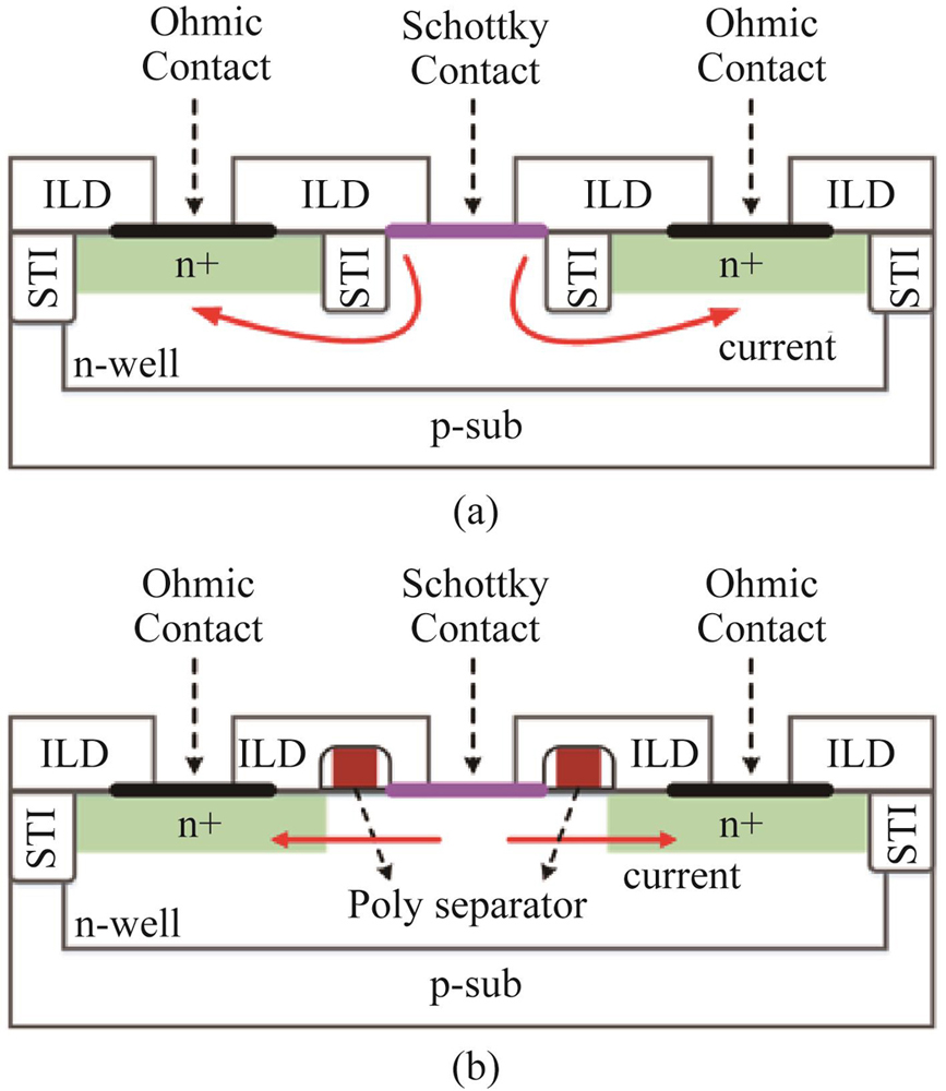
The progress of technology has brought a great leap forward to the overall index of SBD detectors,but the influence of design factors on the index of detectors under the same technology can not be underestimated. There are two main ways to realize Schottky barrier diode in CMOS standard process:shallow trench isolation technology and Polysilicon gate separation technology,shown in Fig. 1. Polysilicon gate separation SBD has less interference to current path,less channel impedance and higher cut-off frequency,which means that it has greater potential in THz imaging field[13].
Figure 1.Structure of two kinds of SBDs (a) shallow trench isolation SBD, (b) polysilicon gate separation SBD
In this paper,we design a high-performance terahertz detector based on self-designed SBD in 180-nm CMOS foundry technology. In Sect.I,the three-dimensional structure of the polysilicon gate separation SBD is built,and the main factors affecting the cut-off frequency of Schottky barrier diode is analyzed and simulated. In Sect. II,we verify and optimize the data according to the results of the tape-out,and find out the technical points of designing a high cut-off frequency diode under the standard CMOS process. In Sect. III,we design a detector with a high-gain on-chip antenna and the key circuit architecture. Then,the terahertz imaging platform is built and the imaging experiment of liquid level detection in wine bottle is completed.
1 Structure analysis of Schottky barrier diodes
The three-dimensional structure of the diode is analyzed in detail to find the design method of high cut-off frequency diodes under the technological limitation,that is particularly important to terahertz detectors. The performance of polysilicon gate separation SBD is better than that of shallow trench isolation SBD in cut-off frequency,which determines our next major analysis of polysilicon gate separation SBD.
As shown in Fig. 2,the polysilicon gate separation SBD separates Schottky contact between metal and lightly doped N-well and Ohmic contact between metal and heavily doped N-well by polysilicon ring.
Figure 2.The three-dimensional structure and two-dimensional profile of polysilicon gate separation SBD
Rs is series resistance and C0 is diode capacitance at zero bias. The expressions of Rs and C0 are derived as below. Individual components contributing to Rs and C0 are shown in Fig. 2.
,,,
where,Rv is the vertical component of R1,Rnwell is n-well sheet resistance, Rpoly is the n-well sheet resistance under the poly separation ring,Rn+ is salicide n+ sheet resistance,Rc is the overall of resistance of vias and contacts,ND is n-well doping density,εSi is the permittivity of silicon,ΦB is the built-in potential,and Cpis the parasitic capacitance of metal terminals. The factor of 1/28.6 is derived from the base-spreading resistance model in Ref.[14]. In addition,ls is the side length of square Schottky contact,l1 is the width of polysilicon ring,l2 is the length of polysilicon to cathode metal contact. The coefficients 1/4 and 1/2 in Eq.3 correspond to the parallel calculation of 4 polysilicon ring and 2 cathode metal in the diode structure diagram,respectively.
From the above analysis,we can get that ls is approximately inversely proportional to the cut-off frequency,that is,smaller anode contact area can get higher cut-off frequency,which is described in many articles. Owing to the obvious limitation of technology on ls and l1,our main research objectives are l2 and l3,which only affects a part of the total resistance and capacitance. And their changes have the opposite effect on the resistance and capacitance values,that requires us to reverse design according to the actual results.
The simulation results of l2 and l3 using Sentaurus and HFSS software with fixed N-well size are shown as Fig. 3. Rx and Cx respectively represent the total resistance and the parasitic capacitance Cp between the positive electrodes and negative electrodes. The length of l3 determined by the number of vias in the negative electrode cannot be continuously changing due to process limitation. In Fig. 3,via X indicates that the negative electrode consists of X vias. As we can see from Fig. 3,with the increase of l2,the resistance will increase and the capacitance will decrease,while l3 has the opposite effect. It is important to observe that this change is not linear,which shows that the effect of l2 on parasitic capacitance decreases when l2 increases to 1.4 μm,and the effect of l3 on resistance can be neglected when the number of vias reaches 7. So far,we cannot determine the optimal size of the SBD,because the simulation results are only a part of the total resistance and capacitance of the SBD. Next,we need to take the changed part into the total impedance and capacitance,and then substitute it into Eq.1 to get the most suitable size of the SBD.
Figure 3.Simulation result of the effect of l2 and l3 on resistance and capacitance (a) capacitance curve, (b) resistance curve
The designed SBDs are fabricated in SMIC 180 nm process,shown in Fig. 4. The DC characteristics are measured by using Agilent B1500A semiconductor parameter analyzer,and the S-parameters are measured by using Agilent E8363B vector network analyzer. When ls and l1 take the minimum value of process,l2=1.4 μm and l3=via5,the series resistance(Rs)and diode capacitance(C0)of 8 SBD are 20 Ω and 10 fF respectively measured by open-short method[15]. The test results of eight parallel SBD are shown in Fig. 5.
Figure 4.Chip physical photo and the SBD plane diagram
Based on the measured results,the simulation results are brought into the above results and normalized to calculate the cut-off frequency FT,which represents the ratio of the cut-off frequency to the cut-off frequency at l2=1.4 μm and l3=via5,shown in Fig. 6.
As we can see from Fig. 6,the diode has the highest cut-off frequency in the current process when l3 is via1 and l2 is between 1 μm to 2 μm. According to Eq.1,the cut-off frequency is about 800 GHz when l2=1.4 μm and l3=via5,and the optimal design scheme can reach about 1 THz when l3=via1 and l2=1~2 μm.
The comparison of previous work is shown in Table. 1. It can be seen that the work of this paper is on the leading level in same technology. But the cut-off frequency of diode will be greatly improved with the improvement of technology,which also indicates that CMOS technology has great potential in terahertz field.
3 The detector and imaging test
The detector consists of on-chip antenna,matching circuit and SBD,shown in Fig. 7. The silicon lens used to further increase gain is packaged with the chip forming the final imaging unit. It is calculated through testing that the antenna gain at 220 GHz is 32 dB,in which the contribution of lens is about 22 dB. The tested responsivity of the detector could achieve 130 V/W and the noise equivalent power is estimated to be 400 pW/.
Figure 7.Photographs of the detector package box and the Chip
Figure 8 shows the imaging test setup and the photo of imaging platform using the designed detector. A multiplier chain driven by signal source(Agilent E8257D)forms terahertz transmitter. When the output power of the signal source is 14 dBm,the maximum output power of the multiplier chain is 12 dBm. A detector is used to receive THz waves passing through the target. And a lock-in amplifier measures the rms value of output voltage for the detector and generates 100 KHz signals for amplitude-modulation(AM)at 220 GHz. The DC drifts and low frequency noise 1/f are eliminated.
Figure 8.Imaging test system (a) the 220 GHz imaging test setup, (b) the photo of 220 GHz imaging platform
In the same process,polysilicon gate separation SBD has higher cut-off frequency than shallow trench isolation SBD. When designing polysilicon gate separation SBD in SMIC 180 nm process,the number of vias in cathode should be as few as possible to increase cut-off frequency. For polysilicon gate separation SBD,when the number of vias constituting the cathode is 1 and the distance between the cathode and the polysilicon is 1~2 μm,the cut-off frequency is the highest,which is about 1 THz. The liquid level imaging experiment in ceramic bottle proves that THz wave has great potential in invisible object detection for its good penetration.