Haitao Luan, Xi Chen, Qiming Zhang, Haoyi Yu, Min Gu. Artificial Intelligence Nanophotonics: Optical Neural Networks and Nanophotonics[J]. Acta Optica Sinica, 2021, 41(8): 0823005
Search by keywords or author
- Acta Optica Sinica
- Vol. 41, Issue 8, 0823005 (2021)
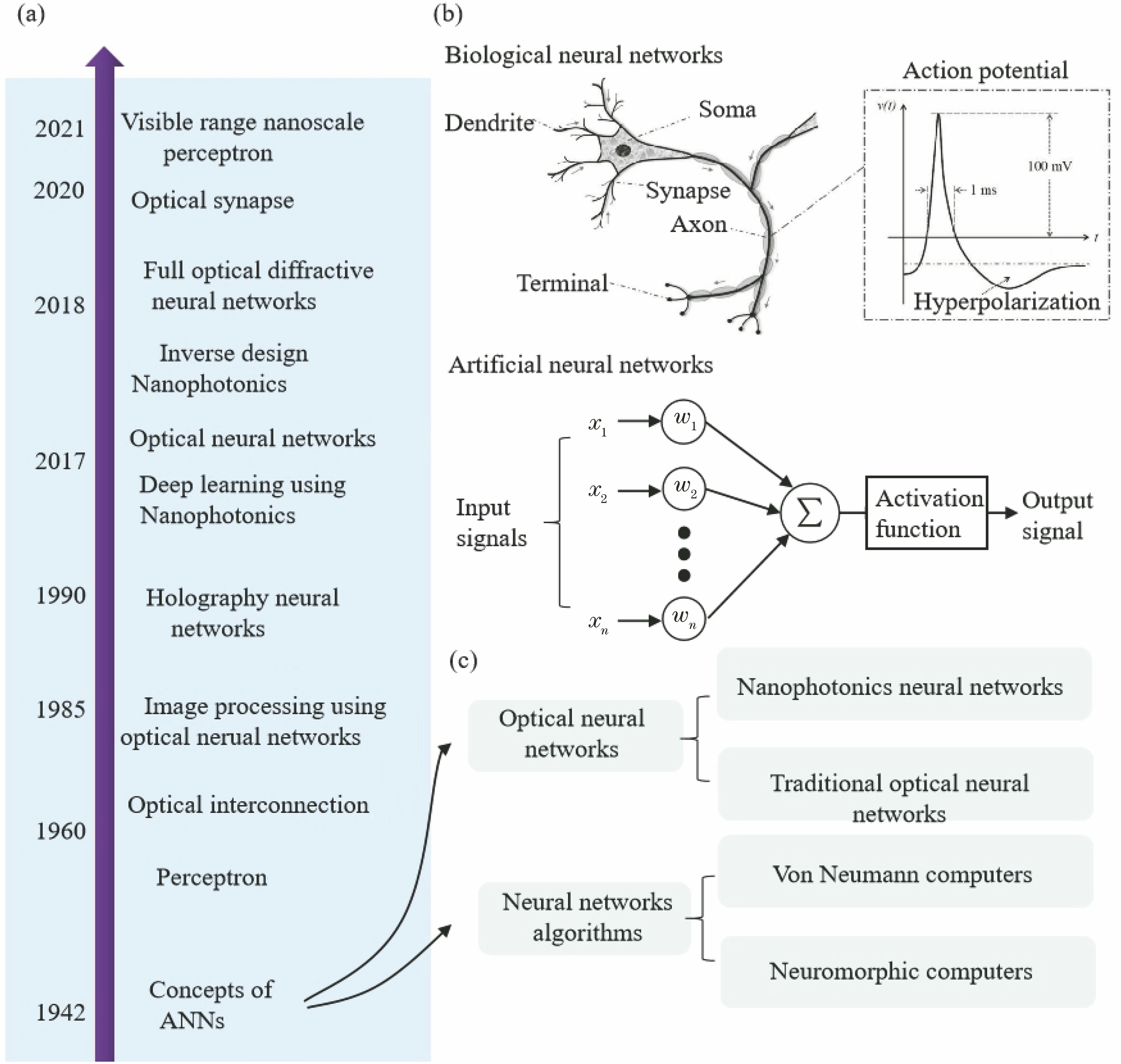
![Concepts of artificial neural networks, and development timeline of optical neural networks. (a) Development timeline of optical neural networks; (b) features of structures and signals of biological neural networks[18] and basic principle of artificial neural networks (x1, x2, and x3 represent input signals, and w1,w2, and wn represent calculation weights); (c) general categories of artificial neural networks](/richHtml/gxxb/2021/41/8/0823005/img_1.jpg)
Fig. 1. Concepts of artificial neural networks, and development timeline of optical neural networks. (a) Development timeline of optical neural networks; (b) features of structures and signals of biological neural networks[18] and basic principle of artificial neural networks (x1, x2, and x3 represent input signals, and w1,w2, and wn represent calculation weights); (c) general categories of artificial neural networks
![Optical neural networks based on traditional optical devices. (a) Holography neural network[32]; (b) optical neural network based on spatial light modulator[34]](/richHtml/gxxb/2021/41/8/0823005/img_2.jpg)
Fig. 2. Optical neural networks based on traditional optical devices. (a) Holography neural network[32]; (b) optical neural network based on spatial light modulator[34]
Fig. 3. Examples of nanophotonics neural networks based on micro/nano optical waveguides. (a) Prototype of optical neural network and experimental diagram[37] (left: principle diagram; middle: experimental configuration; right: signal transmission image and scanning electron microscopic image of experimental setup); (b) structural design of a novel computing chip using optical signal as carrier[38] (top-left: schematic diagram of artificial neural network, which includes input layers, hidden layers, and output layers; top-right: layered demonstration of artificial neural network; bottom: full optical integratable neural networks)
Fig. 4. Examples of nanophotonics neural networks based on diffractive elements. (a) Diffractive neural networks[39](left: diffractive neural networks based on multi-layer transitive/reflective structures; right: experimental demonstration of training process using multi-layer diffractive neural networks); (b) schematic diagram of multi-layer photonic chip intergrated with CMOS fabricated by two-photon 3D laser etching technique[45] ( middle: diagram of two photon laser processing using galvanometer scanning; right: inner structure of multi-layer nanoscale diffractive neural networks. The smallest resolution is 10 nm)
Fig. 5. Examples of inverse designs of topology optimization methods. (a) Inverse design of Z-shape photonic crystal waveguide by topology optimization method[58]; (b) inverse design of wavelength splitter by gradient descent method[59]; (c) inverse design of polarization beam splitter by direct search method[60]
Fig. 6. Examples of design of plasmonic devices based on multi-layer perceptron. (a) Plasmonic nanostructures designed using deep learning model based on bidirectional multi-layer perceptron[65]; (b) inverse design of chiral metamaterials designed using bidirectional multi-layer perceptron neural network[66]
Fig. 7. Switch between long-term and short-term memory modes of photonic synapses under adjustment of number of pulses and frequency[73]. (a) Change of number of pulses; (b) change of frequency
Fig. 8. Paired-pulse facilitation of photonic synapses[73]. (a) Current change curves; (b) relationship between PPF efficiency (A2/A1) and pulse interval
Fig. 9. Learning-experience behavior of photonic synapses[73]. (a) 1st learning; (b) 1st forgetting; (c) 2nd learning; (d) 2nd forgetting
Fig. 10. Plasticity of photonic synapses achieved based on excitation post synaptic currents and inhibition post synaptic currents (tuning applied electric voltage)[73]
Fig. 11. Structures and performances of photonic synapses. (a) Photonic synapses based on indium gallium zinc oxides (left), and curve of electric current change under optical pulse excitation (right)[83]; (b) principle of conductivity control of photonic synapses based on CH3NH3PbI3 driven by photovoltalic effect[89]; (c) structure of photonic synapses based on light induced grating control effect using carbon nanotubes (left) and electric current change curve (right)[93]

Set citation alerts for the article
Please enter your email address


