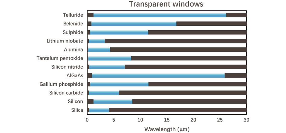
Fig. 1. Infrared transmission window of some materials
[25-29] Fig. 2. Surface topographies of ChG films deposited by different methods. (a) AFM image of GeAsSe films deposited by magnetron sputtering
[69]; (b) optical microscopy image of Ge
2Sb
2Te
5 thin film deposited by fs-PLD
[65]; (c) AFM image of As
33S
67 film fabricated by sol-gel process
[70]; (d) As
2S
3 films deposited on SiO
2 microdisks by thermal evaporation
[66]; (e) 4 inch Ge
25Sb
10S
65 film fabricated by thermal evaporation
[67]; (f) As
55S
45 film fabricated by PECVD
[68] Fig. 3. Morphology images of ChG waveguides obtained by different waveguide fabrication methods. (a) SEM images of Ge
22As
20Se
58 waveguide fabricated by direct laser writing
[71]; (b) schematic of 80GeS
2-15Ga
2S
3-5Sb
2S
3 waveguide fabricated by He
+ ions implanting
[85]; (c) SEM images of As
2S
3 waveguide fabricated by thermal printing
[76]; (d) SEM image of As
2Se
3 waveguide fabricated by wet-etching
[86]; (e) AFM image of Ge
23Sb
7S
70 waveguide fabricated by lift-off
[80] Fig. 4. Morphology images of ChG waveguides fabricated by dry-etching method. (a) Schematic of As
2S
3 waveguide pre-patterned and redeposited on SiO
2 substrate
[66]; (b) SEM image of Ge
23Sb
7S
70 waveguide prepared with SF
6 as etching gas
[91]; (c) SEM image of Ge
23Sb
7S
70 waveguide prepared with chlorine as etching gas
[92]; (d) SEM image of Ge
23Sb
7S
70 waveguide prepared with CHF
3/CF
4 as etching gas
[93]; (e) SEM image of As
2S
3 waveguide prepared with CF
4/O
2 as etching gas
[94]; (f) SEM images of Ge
25Sb
10S
65 waveguide sidewall prepared with and without optimized parameters of Ar/CHF
3/CF
4/O
2[53] Fig. 5. Applications of integrated ChG devices in ultrabroad wavelength regions. (a) Narrow bandwidth Bragg grating filter based on chalcogenide glass in 1.55 μm band
[109]; (b) graphene waveguide integrated detector in 2 μm band
[115]; (c) schematic of photon aerosol spectrometer module in 3 μm band
[116]; (d) schematic of hybrid integrated detector based on spiral chalcogenide waveguide and PbTe film directly integrated under chalcogenide waveguide
[112]; (e) cross-section structure and (f) transmission spectrum of As
2Se
3 waveguides in mid-infrared band
[83]; (g) optical microscope image of spiral single-mode ChG waveguide detector and (h) absorption spectra of methane and nitrous oxide based on device in 7-9 μm wavelength region
[117] Fig. 6. Applications of ChG phase change material-based photonic integrated devices. (a) Optical switch based on Si
3N
4 microresonator and GST
[118]; (b) 1×2 and 2×2 phase change material-based optical switchs
[122]; (c) GSST based polarization rotary optical switch
[125]; (d) working principle and multi-level signal processing of all-optical on-chip memory device
[127]; (e) GST based photonic memory cell and photonic structure of matrix-vector multiplication
[128]; (f) photonic tensor cores for convolution operations
[8]; (g) optical switches based on symmetric and asymmetric microring resonators
[129] Fig. 7. Results of ChG optical waveguides fabricated by laser direct writing method
[132]. Optical microscope images of (a) unexposed area, (b) single straight waveguide, and (c) Y-coupler on ChG film; (d) top view of microring resonator obtained by optical microscope
[133]; (e) fabrication schematic of optical Bragg grating through interference caused by dislocation of shadow masks
[134] Fig. 8. Results of mode splitting caused by photorefractive in ChG microresonators
[136]. (a) Optical microscope image of ChG microresonator; (b) schematic of Bragg grating in ChG microresonator; (c) pattern splitting results caused by different irradiation time; (d) variation curves of mode splitting width Δ
λsplit and corresponding Bragg grating reflectivity
rB with exposure time; (e) reflection spectra of "writing" and "erasing" selected mode in As
2S
3 microcavity based on photoinduced refractive index variation
[137] (upper image is reflection spectrum including three modes, lower left image is reflection spectrum of three modes after erasing mode 2, lower middle image is local reflection spectrum before erasing mode 2, and lower right image is local reflection spectrum after erasing mode 2)
Fig. 9. Hybrid integrated ChG-based devices. (a) ChG and lithium niobate hybrid integrated microring modulator and MZI modulator
[139]; (b) As
2S
3 vertically integrated optical phased array on lithium niobate substrate
[141]; (c) acoustooptic modulator with lithium niobate/GeSbS hybrid integrated MZI structure
[144]; (d) GeSbSe waveguide integrated black phosphorus photodetector
[147]; (e) hybrid integrated photodetector based on ChG waveguide and tellurene
[148] Fig. 10. ChG waveguides and systems for all-optical signal processing
[154]. (a) Cross section of As
2S
3 planar waveguide; (b) simulated group velocity dispersion of TE and TM modes and material dispersion of on-chip waveguide; (c) principle diagrams of transmitter optimization of Tbit/s bandwidth signal and demultiplexing time division multiplexing signal receiver system
Fig. 11. Results of ChG integrated microresonators in optical parametric oscillation applications. (a) Optical parametric oscillation based on As
2S
3 microring resonators
[30];(b) measured threshold power of optical parametric oscillation process (about 5.4 mW)
[30]; (c) four-wave mixing effect based on Ge
11.5As
24Se
64.5 microring resonators
[158]; (d) measured conversion efficiency of four wave mixing as a function of input pump power
[158] Fig. 12. Results of ChG integrated microresonators in optical frequency comb applications
[53,67]. (a) SEM of GeSbS microresonator;(b) bright soliton microcomb; (c) dark-pulse microcomb; (d) Raman-Kerr microcomb
Fig. 13. Results of ChG integrated waveguides in SBS applications. (a) SEM of As
2S
3 rib waveguide; (b) 52 dB Brillouin on-off gain spectrum of As
2S
3 rib waveguide
[164]; (c)(d) As
2S
3-silicon hybrid integrated waveguide and its Brillouin gain spectrum
[165]; (e)(f) As
2S
3-Ge∶SiO
2 hybrid integrated waveguides and its Brillouin gain spectrum
[167]; (g)(h) Ge
25Sb
10S
65 waveguides and its Brillouin gain spectrum
[168]; (i)(j) As
2S
3 waveguides with BCB cladding and its Brillouin gain spectrum
[169] Fig. 14. Applications of SBS in ChG integrated chips. (a) Microwave photonics filters
[171-174]; (b) low-noise microwave source
[175]; (c) microwave measurement
[176]; (d) narrow linewidth on-chip Brillouin laser
[66,165] ; (e) high spatial resolution sensing
[177]; (f) photonic memory
[179] Fig. 15. Large bandwidth tunable ChG-based integrated Raman laser
[53]. (a) SEM of GeSbS microresonator; (b) Raman laser spectrum; (c) output power of the first-order Raman laser as a function of pump power; (d)(e) discrete tuning of the first Stokes output spectrum and discrete tuning of power; (f) discrete tuning of second-order Stokes output spectrum; (g) continuous tuning of Raman laser at different temperatures
Fig. 16. Integrated Raman soliton laser based on ChG waveguides
[182]. (a) Optical microscope image and SEM image of fabricated device with varying waveguide width between 800 and 1000 nm; (b) diagram of experimental setup; (c) measured optical spectra of Raman solitons; (d) Raman soliton spectrum under 7.73 pJ pulse energy; (e) Raman soliton pulse train; (f) autocorrelation trace of Raman soliton single pulse; (g) frequency domain analysis of Raman soliton
| Material | Geometry | n2 /(10-18 m2·W-1) | Loss /(dB·cm-1) | Qint /106 | TPA /(m·W-1) |
|---|
| As2S3[30] | Waveguide | 3 | 0.1 | — | Negligible | | Ge11.5As24Se64.5[31] | Waveguide | 8.6 | 2.6 | — | 10-13 | | Ge22Sb18Se60[32] | Waveguide | 5.1 | 4 | — | 4×10-13 | | Si[33] | Waveguide | 6 | 4 | — | 5×10-12 | | AlGaAs[34-36] | Waveguide | 14.3 | 3.2 | — | 5×10-12 | | LiNbO3[37] | Microring | 0.18 | — | ~4 | Negligible | | SiC[38] | Microdisk | 0.8 | — | 7.1 | Negligible | | Si3N4[39-40] | Microring | 0.25 | — | 422 | Negligible | | AlN[41] | Microring | ~0.35 | — | 1.1 | Negligible | | GaN[42] | Microring | 1.4 | 0.24 | 1.8 | Negligible | | GaP[43] | Microring | 11 | 1.2 | 2 | Negligible |
|
Table 1. Nonlinear optical parameters of some materials at 1.55 μm
Material type | Fabrication method | Refractive index | Dimension | Loss or Q factor |
|---|
Ge23Sb7S70 waveguide[96] | TE RIE | 2.18 | 0.8 μm(width)× 0.42 μm(height) | 0.5 dB·cm-1 | Ge23Sb7S70 microdisk[93] | TE RIE | 2.22 | 0.8 μm×0.45 μm | 1.2×10⁶ | | Ge11.5As24Se64.5 nanowires[31] | TE ICP(inductive coupled plasma)-RIE | 2.66 | 0.63 μm×0.5 μm | 2.6 dB·cm-1 | Ge11.5As24Se64.5 microdisk[97] | TE RIE | 2.545 | 1 μm height | 1.1×10⁶ | Ge25Sb10S65 microring[67] | TE ICP-RIE | 2.2 | 2.4 μm×0.8 μm | 1.3×10⁶ | Ge28Sb12Se60 microdisk[98] | TE ICP | 2.8 | 1 μm height | 5 ×10⁵ | Ge28Sb12Se60 microring[99] | TE ICP | 2.8 | 0.3 μm height | 4.1 ×10⁵ | As20S80 resonator[88] | Micro-trench EBE(electron beam evaporator) | 2.1658 | 2.0 μm×1.5 μm | 6×10⁵ | As2S3 resonator[66] | Trapezoidal- TE | 2.43 | 10 µm×1.3 µm | 1.44×10⁷ | As2S3 microring[100] | Micro-trench TE | 2.45 | 2.5 μm×1.4 µm | 4.6×10⁵ |
|
Table 2. Parameters of chalcogenide optical waveguide and microresonator at 1.55 µm
| Wavelength /μm | Material type | Fabrication method | Refractive index | Dimension | Loss or Q factor |
|---|
| 3.8-5 | Ge11.5As24Se64.5 waveguide[101] | TE ICP | — | 4.0 μm(width)×4.4 μm(height) | ~0.6 dB·cm-1 | | 5.2 | Ge23Sb7S70 microdisk[102] | TE Lift-off | ~2.1 | 3 µm×1.3 µm | 4×10⁵ | | 2.5-6.6 | Ge11.5As24Se64.5 waveguide[103] | TE ICP | 2.609 | 4 µm×1.25 µm | ~0.5 dB·cm-1 | | 2 | As2S3 waveguide[104] | TE ICP | 2.42 | 1.2 μm×0.6 µm | 1.45 dB·cm-1 | | 5.2 | As2S3 microdisk[83] | TE Lift-off | 2.66 | 2.5 μm×1.1 μm | 2×10⁵ | | 2.4 | As2Se3 waveguide[105] | Sputtering Lift-off | 2.79 | 10 μm×1 μm | 0.16 dB·cm-1 | | 8.4 | As2Se3 waveguide[71] | TE Wet etching | 2.78 | 5.4 μm×4.53 μm | 0.5 dB·cm-1 |
|
Table 3. Parameters of chalcogenide optical waveguide and microresonator in mid-infrared band
| Material | Length /cm | Loss / (dB·cm-1) | Brillouin frequency /GHz | Gain, GB /(m-1·W-1) | Pump power /mW | On/off gain /dB |
|---|
| As2S3[163] | 7 | 0.4 | 7.7 | 310.87 | 300 | 18.8 | | As2S3[170] | 7 | 0.4 | 7.7 | 317.39 | 300 | 25.8 | | As2S3[164] | 23 | 0.5 | 7.6 | 500 | 350 | 52 | | As2S3-Si[165] | 5.8 | 0.7 | 7.6 | 750 | 180 | 22.5 | | As2S3-Ge∶SiO2[167] | 23 | 0.5 | 7.8 | 419 | 158 | ~23 | | Ge25Sb10S65[168] | 7 | 0.2 | 7.443 | 338 | 200 | 17.6 | | aAs2S3-Si[166] | 0.8 | 1 | 7.585 | 280 | 100 | - | | As2S3-BCB[169] | 7.5 | 0.2 | 7.75 | 171 | 120 | 5.95 |
|
Table 4. Comparison of Brillouin gain characteristics of integrated chalcogenide waveguides
![Infrared transmission window of some materials[25-29]](/richHtml/gxxb/2022/42/23/2313001/img_01.jpg)
![Surface topographies of ChG films deposited by different methods. (a) AFM image of GeAsSe films deposited by magnetron sputtering[69]; (b) optical microscopy image of Ge2Sb2Te5 thin film deposited by fs-PLD[65]; (c) AFM image of As33S67 film fabricated by sol-gel process[70]; (d) As2S3 films deposited on SiO2 microdisks by thermal evaporation[66]; (e) 4 inch Ge25Sb10S65 film fabricated by thermal evaporation[67]; (f) As55S45 film fabricated by PECVD[68]](/richHtml/gxxb/2022/42/23/2313001/img_02.jpg)
