Abstract
We report the preparation and photoresponse of MoS2 films with different layers grown on c-Al2O3 by pulsed laser deposition (PLD). The phonon modes and crystallographic orientation discussed by Raman scattering and X-ray diffraction (XRD) prove that the MoS2 films are of pure 2H-phase. The S/Mo ratio of film is identified as 1.92:1 derived by X-ray photoelectron (XPS) experiments. The blue and red shifts of the Mo 3d peaks for XPS data indicate the existence of oxidation and sulfur defects in the films. Moreover, by Raman and photoluminescence (PL) mapping, the film thickness is proven to be uniform. The temperature-dependent photoresponse of monolayer MoS2 film indicates that the temperature plays an important role in the photoresponse intensity and response time. The present results can provide a reference for further improving the performance of MoS2-based photodetectors.Introduction
Since graphene has been found, two-dimensional materials as promising materials for next-generation semiconductor devices have been studied and applied in many fields. Among them, transition metal dichalcogenides(TMDs) materials attracted lots of attention with their unique properties[1-2]. MoS2 was one of the TMDS with a direct band gap of about 1.9 eV in monolayer and an indirect bandgap of about 1.3 eV in bulk, which makes it possible in optoelectronic applications[3-4].
As we know, optoelectronic devices have a wide range of applications in every corner of life, such as photodetectors, solar cells, and light-emitting diodes. The thickness of monolayer MoS2 is less than 1 nm, which can be applied in low-dimensional optoelectronic devices. Although chemical vapor deposition(CVD) is the most widely used method for growing two-dimensional materials, other alternative methods are employed at the same time, such as magnetron sputtering[5], atomic layer deposition[6], spin-coating[7], and so on. The pulsed laser deposition(PLD) method can prepare films with the same stoichiometric ratio as the target[8]. As one of the physical vapor deposition methods, PLD was also tried to fabricate large-scale, high-crystallinity and stable-output MoS2 and other 2D films. Many previous work has proved PLD is a practical method for growing two-dimensional materials[9-14].
Sapphire is a commonly used insulating substrate with good optical, mechanical properties and chemical stability. Growing MoS2 films on sapphire substrates is valuable for applications of MoS2. Xu et al. reported wafer-scale MoS2 films on sapphire substrates prepared by a two-step vapor-solid phase reaction process and focused on their electrical performance[15]. Also, some people have employed PLD to grow MoS2 films on sapphire substrates directly and studied their morphology and structure, but not paying attention to the photoresponse[16-17]. Jiao et al. reported preparing high quality MoS2 films with different thicknesses by PLD and investigated the layer-dependent photoresponse ranging from UV-visible-NIR spectra[18], but the influence of temperature is not considered. Note that, the temperature affects the stability of the device operation. As we know, temperature will cause the expansion or contraction of the crystal lattice, which will change the phonon vibration and electronic structure of the crystal[19-20]. We think this will affect the photoelectric properties of the crystal. If the MoS2 films are to be used in optoelectronic devices, the effects on the photoresponse from the temperature must be considered. Studying the effects of temperature on photoresponsivity and response time is necessary. Therefore, in this paper, we prepared MoS2 films with different layers directly using PLD technology. Then, we investigated the structure, composition, uniformity and the photoresponse in different situations.
1 Experiments
A commercial target was placed 5.5 cm in front of the substrates with S/Mo ratio of 2:1. A pulsed 248 nm KrF excimer laser was used to etch the surface of the target. The energy fluence is set to 4 Jcm-2 with a repetition rate of 5 Hz. Before placed in the vacuum chamber, the square sapphire substrates with a thickness of 0.5 mm were cleaned in alcohol, acetone, and deionized water for 15 minutes separately, combined with sonication. During the deposition, the chamber was kept at a vacuum of 5×10⁻⁶ mba. Simultaneously, the heater was kept at 800 ℃ and rotated to improve the flatness of the films. The thicknesses of the films are controlled by the repetition number of the laser pulses. Due to the volatility of sulfur, each sample was immediately placed in a double-temperature zone tube furnace and annealed in a sulfur atmosphere after being taken out of the PLD vacuum chamber. During the annealing progress, the samples were heated at 700 ℃ and the excess sulfur was heated at 200 ℃ with an argon flow rate of 100 sccm.
The thickness and the roughness were identified by atomic force microscopy(AFM, digital Instruments Icon, Bruker). The phonon changes and photoluminescence of the samples were studied by Raman spectroscopy(Jobin-Yvon LabRAM HR Evolution) using a 50× lens with an excitation laser beam wavelength of 532 nm. X-ray photoelectron spectroscopy(XPS, RBD upgraded PHI-5000C ESCA system, PerkinElmer) measurements were applied to investigate the Mo 3d and S 2p regions of the samples. X-ray diffraction(XRD, D/MAX-2550 V, Rigaku Co) analysis was carried out to investigate the crystalline and compositions. The electrical characteristics and photoresponse were measured by a Keithley model 4200 with gold contacts. A 637nm laser was used as the light source.
2 Results and discussions
2.1 Morphology and structure
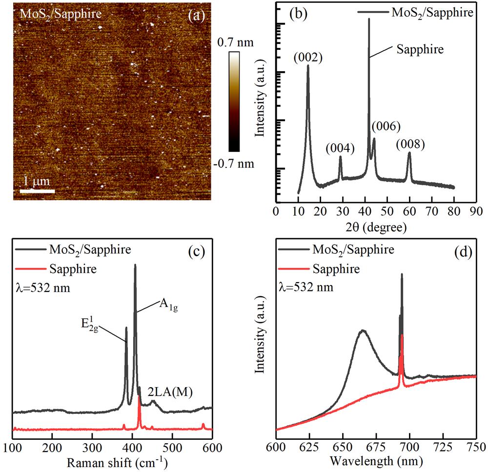
Firstly, the surface morphology was measured by atomic force microscopy(AFM). Figure 1(a) shows the topography of a MoS2 film deposited on a c-Al2O3 substrate. The calculated arithmetic roughness is 0.162 nm, which means that the film has extremely high flatness. The diffraction pattern in Fig. 1(b) for the film has five strong peaks at 14.4º, 29.1º, 41.8º, 44.2º and 60.1º. In addition to the peak at 41.8º belonging to the sapphire substrate, the other four peaks correspond to the(002)(004)(006) and(008) orientations(JCPDS No. 37-1492) of 2H-MoS2, respectively. Besides, there are no peaks belonging to 1T-MoS2. The full width at half maximum(FWHM) of(002) peak is 0.321º, which indicates that the crystallite size of this sample is 25.3 nm estimated by Scherrer formula[D=0.9λ/(βcosθ)]. From the Raman spectra in Fig. 1(c), except for the peaks derived from the substrate, the other 3 main peaks are the in-plane vibration E12g, out-of-plane vibration A1g and the second-order longitudinal acoustic mode at the M point 2LA(M). Note that the E12g and A1g modes are corresponding to the 2H-phase of MoS2. Both the results of XRD and Raman spectra indicate that the MoS2 films in this work is pure in 2H semiconductor phase[21]. A confocal microscope system(Jobin-Yvon LabRAM HR Evolution spectrometer) with a 532 nm laser was adopted to collect the PL data of a film with 150 pulses. As shown in Fig. 1(d), a single strong excitonic peak appears around 665 nm corresponding to a band gap with 1.86 eV, the PL spectrum of sapphire is used as a reference, which suggests that it is a monolayer MoS2 film.

Figure 1.(a) The AFM image of a MoS2 film on a c-Al2O3 substrate, The(b) XRD and(c) Raman spectra of the MoS2 film,(d) The PL spectra of a MoS2 film
X-ray photoelectron spectroscopy(XPS) was used to analyze the stoichiometry and chemical states of the film. The spectra in Fig. 2 is referenced to C 1s emission at 284.6 eV. Fig. 2(a) is the survey spectra of the monolayer exhibit peaks for Mo and S elements as well as the sapphire substrate. Figure 2(b) and Figure 2(c) present the Mo and S core level peak regions, along with the deconvolutions of each spectrum. Some constraints are applied to ensure that the fitting results have a physical meaning. The binding energy differences ΔEB between Mo 3d5/2 and Mo 3d3/2 orbitals, S 2p3/2 and S 2p1/2 orbitals were constrained as(3.1±0.1)eV and(1.2±0.1)eV, respectively. The areas of Mo 3d5/2 and S 2p3/2 orbitals are constrained as 1.5 and 2 times of the Mo 3d3/2 and 2p1/2 orbitals, respectively[14,22]. As shown in Fig. 2(b), the strongest doublet peaks around 232.8 eV and 229.7 eV are attributed to the Mo4+ state of 2H MoS2. The doublet peaks around 236.0 eV and 232.9 eV belong to Mo 3d3/2 and Mo 3d5/2 orbitals of Mo6+ state, which indicates the existence of oxidation. The peak around 226.9 eV is identified as S 2s core level. Additional doublet peaks around 232.1 eV and 229.0 eV red-shifted from the main peaks by 0.7 eV suggest the presence of Mo4+ of other states. Some works have reported that this phenomenon is due to the symbiosis of the 2H-phase and 1T-phase[23]. However, no evidence of the 1T-phase is found according to the results of Raman spectra and XRD. In this work, the sulfur defects reduce the actual valence of some Mo elements and increases the electron cloud density, which leads to a reduction in the binding energy of these Mo elements to the electrons[14,16,24]. For S 2p core level, the main peaks corresponding to 2p1/2 and 2p3/2 orbitals are around 163.7 eV and 162.5 eV. Similarly, there is a pair of doublet peaks around 162.8 eV and 161.6 eV red-shifted by 0.9 eV to the main peaks, indicating the presence of other S-2 states, which should be related to sulfur defects and oxidation. Through the areas of the S 2p peaks and Mo 3d peaks, the S/Mo ratio is calculated as 1.92:1.
Figure 2.(a) The survey XPS spectra of a film deposited for 150 pulses, The XPS spectra and its deconvolution of(b) Mo 3d and(c) S 2P core level
2.2 Uniformity analysis
For two-dimensional materials, Raman mapping is often used to evaluate the uniformity of thin films[16,25-26]. As shown in Fig. 3(a), a random 40 μm × 40 μm area was tested for uniformity. The dark areas in the image may be related the particles sputtered from the target. The frequency difference(Δν) between the E12gand A1gmodes of monolayer MoS2, less than 20 cm-1, is known as an indicator for monolayer. Therefore, Raman mapping was applied to measure the uniformity of the film. As shown in Fig. 3(b), most points in the picture have a frequency difference of less than 20 cm-1. After calculation, the average value of the frequency difference is 19.7 cm-1 with the standard deviation of 0.35 cm-1, which suggests that this film has a good uniformity in thickness. The intensity mapping of the A1gmode is also presented in Fig. 3(c). The dispersion of the peak intensity is greater than the frequency difference, which may be due to the difference in crystallinity introduced by defects, grain boundaries, impurities absorbed on surface, etc. At the same time, we suspect that the film is polycrystalline. Similar phenomena can also be found in PL mapping. In Fig. 3(d), the calculated average position value of the excitonic peak is 664.8 nm corresponding to a band gap of 1.87 eV, with a very small standard deviation of 0.29 nm. Similarly, the distribution of the PL intensity in Fig. 3(e) is not as even as the position, but with no dead pixels. Although the crystallinity distribution is not perfect, the MoS2 films grown by PLD can be precisely controlled in thickness. Different layers of MoS2 films were easily prepared, as shown in Fig. 3(f), which can be distinguished by the change in the frequency differences of the E12g and A1g modes. When the thickness increases, the E12g shows a red shift and the A1g modes has a blue shift, which is consistent with previous reports[26-27]. The inerlayer vdW interaction increasing the effective restoring forces acting on the atoms, which is believed to cause the blue shift of A1g mode with increasing layer number. However, the red shift of E12g mode may reflect the influence of stacking-induced structural changes, attributed to long-range Coulombic interlayer interaction[27]. Based on the XRD spectrum, Raman Spectrum, Raman and PL mapping, we speculate that the MoS2 films grown by PLD in this work are pure in 2H-Phase and polycrystalline.
Figure 3.(a) The optical image of a randomly selected 40 μm × 40 μm area,(b) The mapping of the frequency differences between E12g and A1g peaks,(c) The mapping of the intensity of the A1g peak. The mapping of the excitonic peak(d) positions and(e) intensity,(f) The Raman spectra for different layers
2.3 Effect of temperature
As for the optoelectronic properties, 40 nm thick gold electrodes were plated on the films using a mask by thermal evaporation to collect current. The channel between the adjacent electrodes is 50 μm wide and 150 μm long. Figure 4(a) shows the schematic of the photoresponse measurement progress. A 637 nm laser was used to excite the electron from valence band to conduction band. The photon energy of the selected laser is slightly larger than the band gap of monolayer MoS2, so that it does not generate excessive heat under the premise that it can excite electrons from the valence band top to the conduction band bottom. This reduces the influence of the heat generated by the laser on the accuracy of temperature control. Figure 4(b) shows the layer-dependent time-resolved photocurrent of the MoS2 films under the same laser irradiation and driving voltage. Compared the five films, the monolayer sample has a photocurrent of 0.32 nA with a photoresponsivity of about 3 mAW-1, which is stronger than the others. As shown in Fig. 4(c), the layer-dependent rising(τup) and decay response times(τdown) are extracted. The inset of Fig. 4(c) shows the rising and decay response times of the monolayer MoS2 film. The monolayer MoS2 film has the slowest response, which is believed to be related to its direct bandgap. When the number of layers increased to 2 or more layers, the direct bandgap becomes an indirect band gap, which reduces the photo-generated carrier life and response times. To further study the optoelectronic characteristics of the monolayer MoS2 film, the photoresponse at different temperature under vacuum was carried out. Figure 4(d) shows the time-resolved photocurrent at 200 K, 270 K and 370 K. Each one shows good reproducibility at different temperatures after several cycles. The Iphoto and Idark increase synchronously with the temperature, as shown in Fig. 4(e). As the temperature increases, the intrinsic carrier concentration will increase with thermal excitation, which will increase the conductivity of monolayer MoS2 film. So, the photocurrent and dark current both increase with the temperature, and the dark current is more affected by temperature. The study on temperature effects on the electronic structure found that the band gap will decrease monotonously with the temperature[20]. The narrowing of the band gap with the temperature will reduce the difficulty of electron excitation from valence band top to the conduction band bottom. As a result, the photocurrent of this monolayer MoS2 film in the inset of Fig. 4(e) increases as the temperature rises. The τup and τdown are extracted from the temperature-dependent photoresponse data, as shown in Fig. 4(f). When the temperature is lower than 260 K, the response time rises rapidly with the temperature. However, when the temperature is higher than about 280 K, the response time slows down as the temperature rises. The narrowing of the band gap with the temperature will decrease the response times. However, the ionization of defects will increase with temperature, becoming the scattering center of non-equilibrium carriers and increasing the lifetimes of the photo-generated non-equilibrium carriers, which will increase the response times. The change in response time around room temperature may be related to the complex competition between these mechanisms. Such results indicate that the temperature compensation needs to be considered when designing the MoS2-based devices.
Figure 4.(a) The schematic of the photoresponse measurement progress,(b) The time-resolved photocurrent of MoS2 films with different layers,(c) The layer-dependent rising(τup) and decay response times(τdown). The inset presents the rising and decay response times of the monolayer MoS2 film,(d) The time-resolved photoresponse of a monolayer MoS2 film at 200 K, 270 K and 370 K,(e) The temperature-dependent photoresponse of a monolayer MoS2 film. The inset presents the temperature-dependent Iph,(f) The temperature-dependent rising(τup) and decay response times(τdown)
3 Conclusions
In conclusion, we prepared the high-quality and thickness-controllable MoS2 films on the c-Al2O3 substrates using the PLD method. The phonon modes and crystallographic orientation were studied through Raman and XRD spectra, providing evidence for the pure 2H-phase. The XPS results show the existence of oxidation and sulfur defects in the films. By Raman and PL mapping, the thickness is proved good uniformity and the monolayer film is presumed to be polycrystalline. Moreover, we find that the temperature has a great influence on the optoelectronic properties. Our findings should be helpful for designing and producing high-performance MoS2-based photodetectors.
References
[1] B RADISAVLJEVIC, A RADENOVIC, V BRIVIO et al. Single-layer MoS2 Transistors. Nature Nanotechnology, 6, 147-150(2011).
[2] G R BHIMANAPATI, Z LIN, V MEUNIER et al. Recent Advances in Two-dimensional Materials Beyond Graphene. ACS Nano, 9, 11509-11539(2015).
[3] D BURMAN, R GHOSH, S SANTRA et al. Role of Vacancy Sites and UV-ozone Treatment on Few Layered MoS2 Nanoflakes for Toxic Gas Detection. Nanotechnology, 28, 435502-435518(2017).
[4] L WANG, J S JIE, Z B SHAO et al. MoS2/Si Heterojunction with Vertically Standing Layered Structure for Ultrafast, High-detectivity, Self-driven Visible-Near Infrared Photodetectors. Advanced Functional Materials, 25, 2910-2919(2015).
[5] J G TAO, J W CHAI, X LU et al. Growth of Wafer-scale MoS2 Monolayer by Magnetron Sputtering. Nanoscale, 7, 2497-2503(2015).
[6] L K TAN, B LIU, J H TENG et al. Atomic layer deposition of a MoS2 film. Nanoscale, 6, 10584-10588(2014).
[7] J YANG, Y GU, E LEE et al. Wafer-scale Synthesis of Thickness-controllable MoS2 Films Via Solution-processing Using A Dimethylformamide/n-butylamine/2-aminoethanol Solvent System. Nanoscale, 7, 9311-9319(2015).
[8] Z B YANG, J H HAO. Progress in Pulsed Laser Deposited Two-dimensional Layered Materials for Device Applications. Journal of Materials Chemistry C, 4, 8859-8878(2016).
[9] W J JIE, Z B YANG, F ZHANG et al. Observation of Room-temperature Magnetoresistance in Monolayer MoS2 by Ferromagnetic Gating. ACS Nano, 11, 6950-6958(2017).
[10] Y XIE, B ZHANG, S X WANG et al. Ultrabroadband MoS2 Photodetector with Spectral Response from 445 to 2 717 nm. Advanced Materials, 29, 1605972-(2017).
[11] A GOSWAMI, P DHANDARIA, S PAL et al. Effect of Interface on Mid-infrared Photothermal Response of MoS2 Thin Film Grown by Pulsed Laser Deposition. Nano Research, 10, 3571-3584(2017).
[12] C R SERRAO, A M DIAMOND, S L HSU et al. Highly Crystalline MoS2 Thin Films Grown by Pulsed Laser Deposition. Applied Physics Letters, 106, 052101(2015).
[13] A ARULRAJ, M RAMESH, SUBRAMANIAN et al. In-situ Temperature and Thickness Control Grown 2D-MoS2 via Pulsed Laser Ablation for Photovoltaic Devices. Solar Energy, 174, 286-295(2018).
[14] J LIU, A GOSWAMI, K JIANG et al. Direct-current Triboelectricity Generation by A Sliding Schottky Nanocontact on MoS2 Multilayers. Nature Nanotechnology, 13, 112-116(2018).
[15] X M XU, Z W WANG, S LOPATIN et al. Wafer Scale Quasi Single Crystalline MoS2 Realized by Epitaxial Phase Conversion. 2D Materials, 6, 015030(2018).
[16] M I SERNA, S H YOO, S MORENO et al. Large-area Deposition of MoS2 by Pulsed Laser Deposition with In Situ Thickness Control. ACS Nano, 10, 6054-6061(2016).
[17] A BARVAT, N PRAKASH, B SATPATI et al. Emerging Photoluminescence from Bilayer Large-area 2D MoS2 Films Grown by Pulsed Laser Deposition on Different Substrates. Journal of Applied Physics, 122, 015304(2017).
[18] L JIAO, W J JIE, Z B YANG et al. Layer-dependent Photoresponse of 2D MoS2 Films Prepared by Pulsed Laser Deposition. Journal of Materials Chemistry C, 7, 2522-2529(2019).
[19] N A LANZILLO, A G BIRDWELL, M AMANI et al. Temperature-dependent phonon shifts in monolayer MoS2. Applied Physics Letters, 3, 056103(2015).
[20] A MOLINA-SÁNCHEZ, M PALUMMO, A MARNI et al. Temperature-dependent excitonic effects in the optical properties of single-layer MoS2. Physical Review B, 93, 155435(2016).
[21] Y F YU, G H NAM, Q Y HE et al. High Phase-purity 1T′-MoS2- and 1T′-MoSe2-layered Crystals. Nature Chemistry, 10, 638-643(2018).
[22] D J LATE, P A SHAIKH, R KHARE et al. Pulsed Laser-deposited MoS2 Thin Films on W and Si: Field Emission and Photoresponse Studies. ACS Applied Materials& Interfaces, 6, 15881-15888(2014).
[23] A BARVAT, N PRAKASH, G KUMAR et al. Electronic Structure of The PLD Grown Mixed Phase MoS2/GaN Interface and Its Thermal Annealing Effect. Current Applied Physics, 18, 170-177(2018).
[24] X K ZHANG, Q L LIAO, S LIU et al. Poly(4-styrenesulfonate)-induced Sulfur Vacancy Self-healing Strategy for Monolayer MoS2 Homojunction Photodiode. Nature Communications, 8, 15881(2017).
[25] S SEO, S KIM, H CHOI et al. Direct in Situ Growth of Centimeter‐Scale Multi‐Heterojunction MoS2/WS2/WSe2 Thin‐film Catalyst for Photo‐electrochemical Hydrogen Evolution. Advanced Science, 6, 1900301.
[26] G SIEGEL, Y P V SUBBAIAH, M C PRESTGARD et al. Growth of Centimeter-scale Atomically Thin MoS2 Films by Pulsed Laser Deposition. APL Materials, 3, 056103(2015).
[27] C G LEE, H G YAN, L E BRUS et al. Anomalous Lattice Vibrations of Single- and Few-Layer MoS2. ACS Nano, 4, 2695-2700(2010).