• Laser & Optoelectronics Progress
  • Vol. 61, Issue 5, 0504003 (2024)
Haibo Zhang, Ting Ji*, Jiayu He, Linlin Shi, Guohui Li, and Yanxia Cui**
Author Affiliations
  • College of Optoelectronics, Taiyuan University of Technology, Taiyuan 030024, Shanxi, China
  • show less
    DOI: 10.3788/LOP230924 Cite this Article Set citation alerts
    Haibo Zhang, Ting Ji, Jiayu He, Linlin Shi, Guohui Li, Yanxia Cui. Fast-Response Vertical-Structure Two-Dimensional Perovskite Photodetector[J]. Laser & Optoelectronics Progress, 2024, 61(5): 0504003 Copy Citation Text show less
    Structure diagram of vertical structure two-dimensional perovskite photodetector
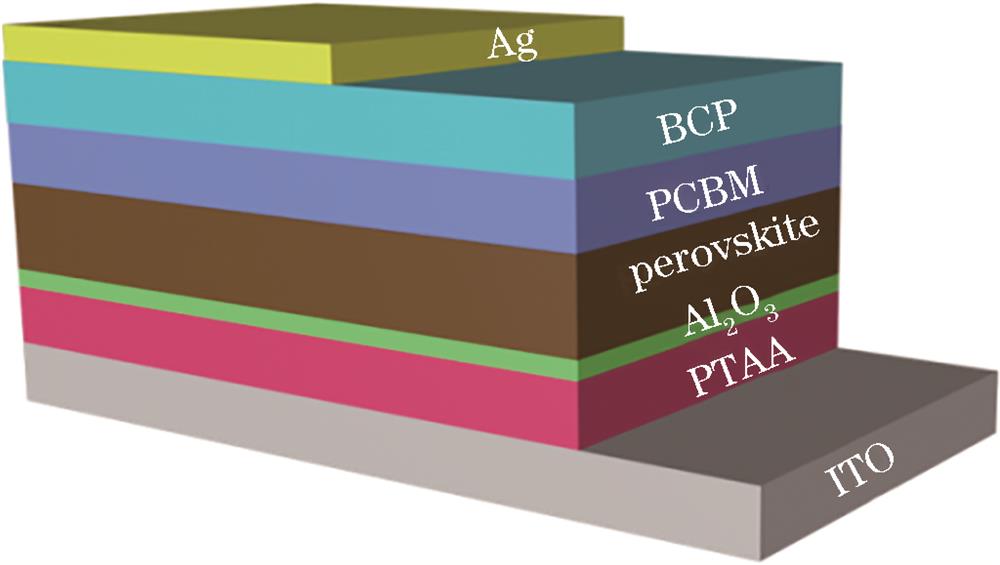
    Fig. 1. Structure diagram of vertical structure two-dimensional perovskite photodetector
    Cross-sectional TEM image of device
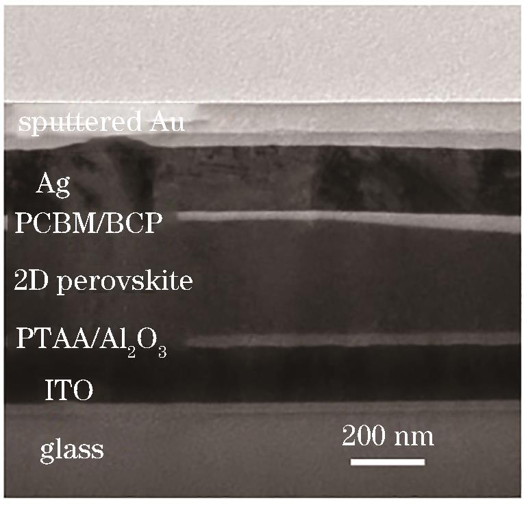
    Fig. 2. Cross-sectional TEM image of device
    XRD patterns of two-dimensional perovskite thin film. (a) No additive; (b) NH4SCN; (c) NH4Cl; (d) NH4SCN and NH4Cl
    Fig. 3. XRD patterns of two-dimensional perovskite thin film. (a) No additive; (b) NH4SCN; (c) NH4Cl; (d) NH4SCN and NH4Cl
    J-V curves of two-dimensional perovskite photodetectors with different thicknesses. (a) In dark state; (b) in laser irradiation
    Fig. 4. J-V curves of two-dimensional perovskite photodetectors with different thicknesses. (a) In dark state; (b) in laser irradiation
    Parameters of two-dimensional perovskite devices with different thicknesses under 0 V bias voltage. (a) fEQE; (b) R0; (c) D*; (d) transient photocurrent curves
    Fig. 5. Parameters of two-dimensional perovskite devices with different thicknesses under 0 V bias voltage. (a) fEQE; (b) R0; (c) D*; (d) transient photocurrent curves
    XRD patterns of two-dimensional perovskite films with different thicknesses
    Fig. 6. XRD patterns of two-dimensional perovskite films with different thicknesses
    AFM surface topographies of two-dimensional perovskite films with different thicknesses (a) 280 nm; (b) 140 nm; (c) 80 nm; (d) 50 nm
    Fig. 7. AFM surface topographies of two-dimensional perovskite films with different thicknesses (a) 280 nm; (b) 140 nm; (c) 80 nm; (d) 50 nm
    Transient photocurrent curves of photodetectors based on different effective areas
    Fig. 8. Transient photocurrent curves of photodetectors based on different effective areas
    Perovskite film thickness /nmτrise/nsτfall/nsτ/ns
    28033564597
    14034533567
    8030422452
    5043730773
    Table 1. Response time of two-dimensional perovskite photodetectors with different thicknesses
    Device structurePhotoactive layerResponse timeMethod
    Lateral-type(BA)2(MA)2Pb3I1010/7.5 msRef.[35
    (BA)2(MA)n-1PbnBr3n+10.21/0.24 sRef.[36
    (BA)2(MA)3Pb4I1352.1 μsRef.[37
    (PA)2(MA)Pb2I71.52/1.67 μsRef.[38
    (BA)2PbI41.7/3.9 μsRef.[39
    (PEA)2SnI434 msRef.[40
    (PA)2(FA)Pb2I70.86/2.54 nsRef.[34
    (BA)2Pb2I7< 4 msRef.[41
    (BA)2(MA)Pb2Br720 μsRef.[42
    (PEA)2PbI421/37 μsRef.[18
    (C6H13NH32(FA)Pb2I7310/520 μsRef.[43
    (PEA)2PbBr40.41/0.37 msRef.[20
    (BA)2(MA)3Pb4I133.53/3.78 msRef.[44
    2D FAPbI30.35/0.54 msRef.[26
    (BA)2CsPb2Br7~300 μsRef.[25
    Vertical-type(PEA)2(MA)4Pb5I1633/564 nsRef.[28
    (PDA)(MA)3Pb4I1320/45 msRef.[21
    (PEA)2(MA)2Pb3I1029/152 nsRef.[27
    (PEA)2(MA)4Pb5I1621/92 nsThis work
    Table 2. Summary of response time of two-dimensional perovskite photodetector
    Haibo Zhang, Ting Ji, Jiayu He, Linlin Shi, Guohui Li, Yanxia Cui. Fast-Response Vertical-Structure Two-Dimensional Perovskite Photodetector[J]. Laser & Optoelectronics Progress, 2024, 61(5): 0504003
    Download Citation