• Photonics Research
  • Vol. 10, Issue 11, 2526 (2022)
Xuan Xiao, Yanxin Lu, Jiayi Jiang, and Yihang Chen*
Author Affiliations
  • Guangdong Provincial Key Laboratory of Quantum Engineering and Quantum Materials, School of Physics and Telecommunication Engineering, South China Normal University, Guangzhou 510006, China
  • show less
    DOI: 10.1364/PRJ.465119 Cite this Article Set citation alerts
    Xuan Xiao, Yanxin Lu, Jiayi Jiang, Yihang Chen. Manipulation of optical bound states in the continuum in a metal-dielectric hybrid nanostructure[J]. Photonics Research, 2022, 10(11): 2526 Copy Citation Text show less
    (A) Schematic illustration of the hybrid metal-dielectric nanostructure. It is composed of a Si NP array arranged in a hexagonal lattice, a thin SiO2 spacer, an Ag film, and a SiO2 substrate. The red arrow represents the direction of incident light. (B) Schematic of a unit cell of the Si NP array. In the following discussions, we choose a=400 nm, d=200 nm, h=190 nm, L1=30 nm, and L2=100 nm.
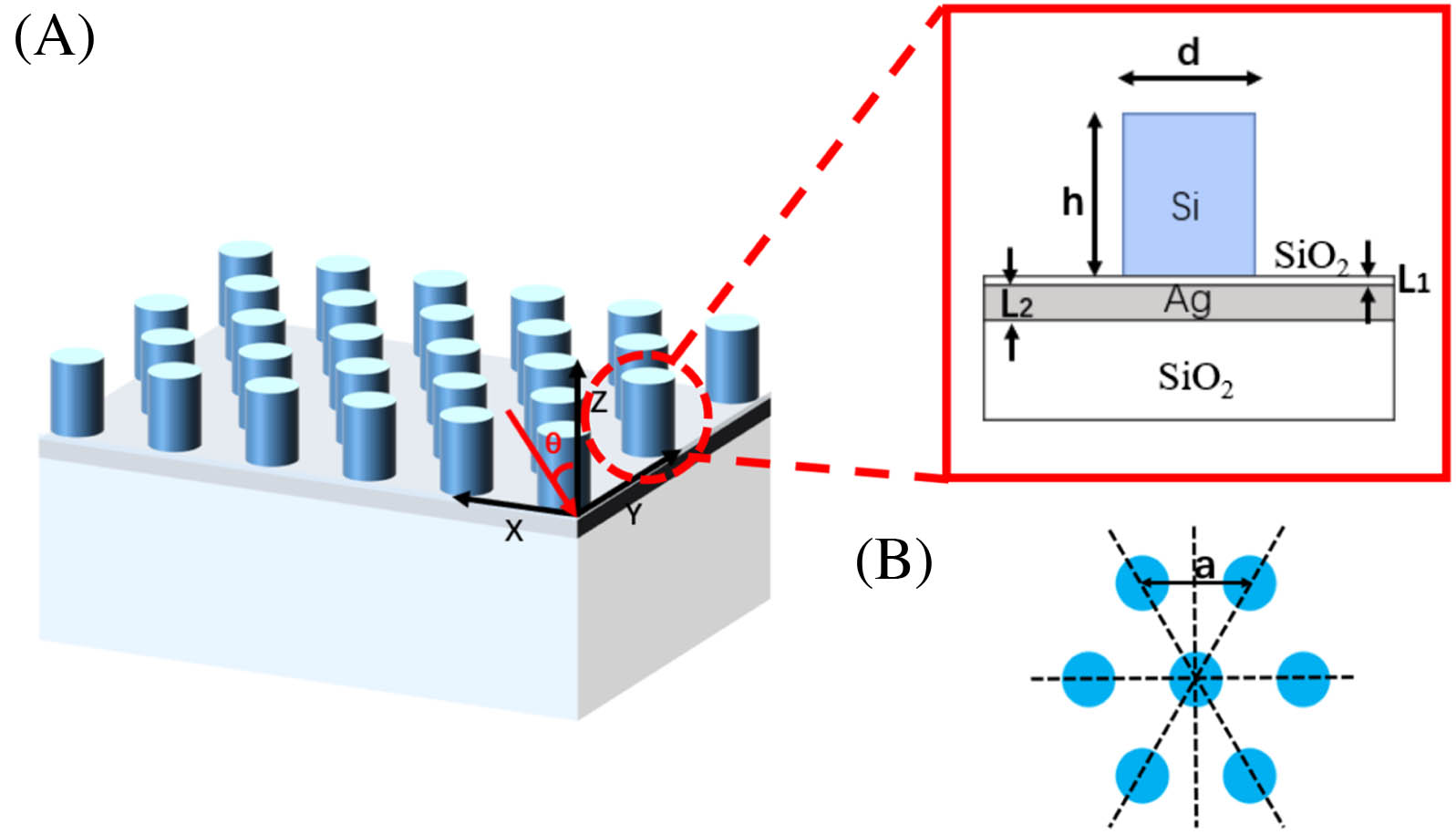
    Fig. 1. (A) Schematic illustration of the hybrid metal-dielectric nanostructure. It is composed of a Si NP array arranged in a hexagonal lattice, a thin SiO2 spacer, an Ag film, and a SiO2 substrate. The red arrow represents the direction of incident light. (B) Schematic of a unit cell of the Si NP array. In the following discussions, we choose a=400  nm, d=200  nm, h=190  nm, L1=30  nm, and L2=100  nm.
    (A) Simulated reflection spectrum of the considered hybrid structure under normal incidence. The two reflection dips at 596 and 746 nm correspond to the SPP and MMD modes, respectively. Electric field distributions in the xz plane (B) at 596 nm and (C) at 746 nm. The arrows represent the electric field vectors. (D) Illustration of the MMD induced from the ED inside a nanoparticle and its mirror image in the metal film.
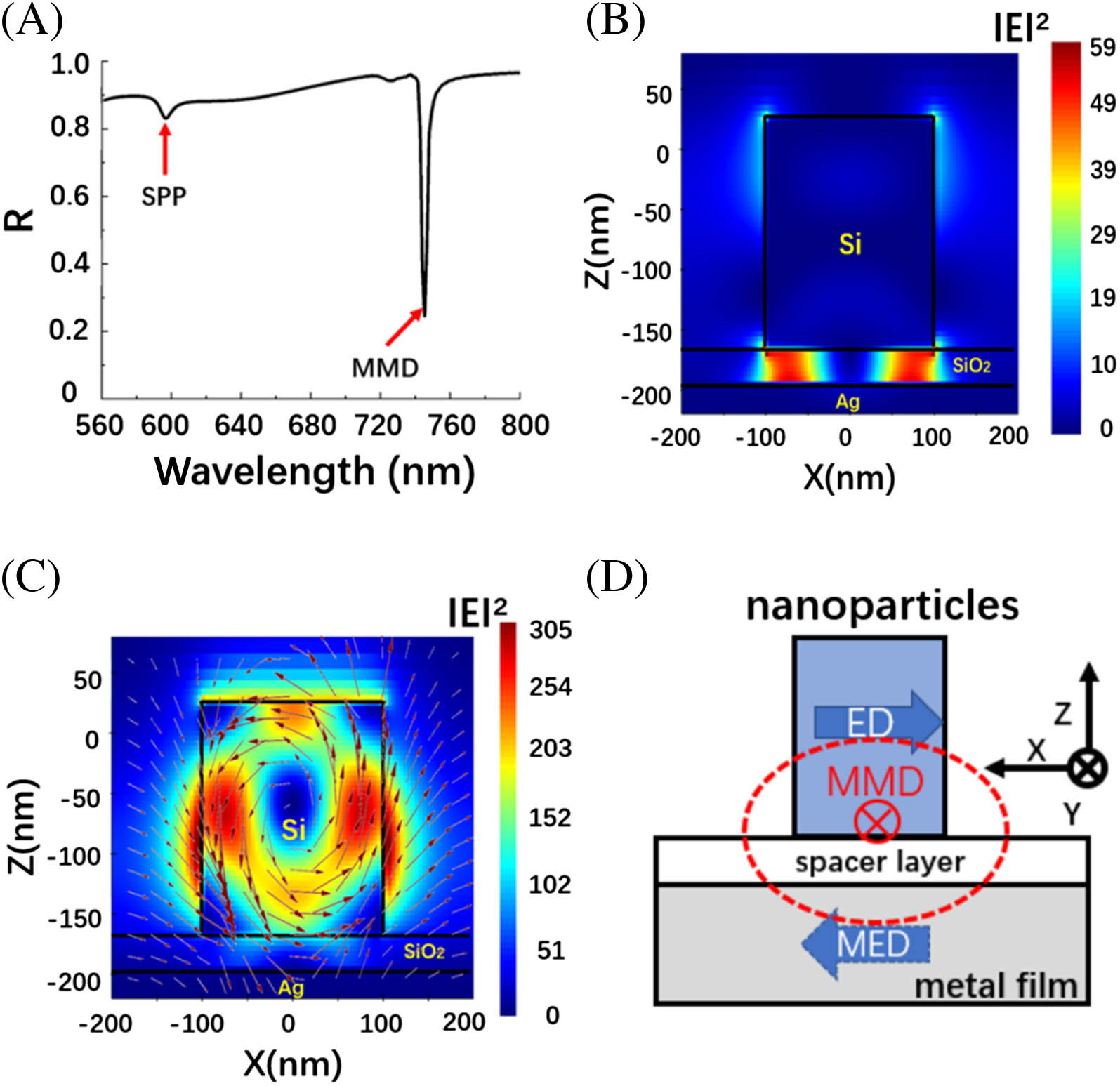
    Fig. 2. (A) Simulated reflection spectrum of the considered hybrid structure under normal incidence. The two reflection dips at 596 and 746 nm correspond to the SPP and MMD modes, respectively. Electric field distributions in the xz plane (B) at 596 nm and (C) at 746 nm. The arrows represent the electric field vectors. (D) Illustration of the MMD induced from the ED inside a nanoparticle and its mirror image in the metal film.
    Reflection spectra of the metal–dielectric hybrid system as a function of incident angle for (A) p- and (B) s-polarized plane waves. The SP-BICs and the accidental BICs are all highlighted by dashed circles. (C) and (D) are the polarized reflection spectra for the structure where Si NP array is placed on a thick SiO2 substrate.
    Fig. 3. Reflection spectra of the metal–dielectric hybrid system as a function of incident angle for (A) p- and (B) s-polarized plane waves. The SP-BICs and the accidental BICs are all highlighted by dashed circles. (C) and (D) are the polarized reflection spectra for the structure where Si NP array is placed on a thick SiO2 substrate.
    Simulated band structures for Si NPs deposited on a thick SiO2 substrate without the Ag film under TM polarization. The structural parameters are the same as those in Fig. 1. Nondegenerate mode at 755 nm and doubly degenerate modes exist at 550 and 585 nm in the Γ-point.
    Fig. 4. Simulated band structures for Si NPs deposited on a thick SiO2 substrate without the Ag film under TM polarization. The structural parameters are the same as those in Fig. 1. Nondegenerate mode at 755 nm and doubly degenerate modes exist at 550 and 585 nm in the Γ-point.
    Simulated electric field distributions in the xz plane for (A) the SPP-coupled quasi-BIC at 632.6 nm in our hybrid structure and (B) the quasi-BIC at 596.5 nm in the all-dielectric structure with an incident angle of 3°; (C) Q factor versus angle of incidence for the SPP-coupled quasi-BIC in hybrid structure (black) and plasmonic structure (red); (D) dependence of the optical mode volume ratio for the SPP-coupled quasi-BIC in hybrid structure (V) and plasmonic structure (V0) on the thickness of the SiO2 spacer.
    Fig. 5. Simulated electric field distributions in the xz plane for (A) the SPP-coupled quasi-BIC at 632.6 nm in our hybrid structure and (B) the quasi-BIC at 596.5 nm in the all-dielectric structure with an incident angle of 3°; (C) Q factor versus angle of incidence for the SPP-coupled quasi-BIC in hybrid structure (black) and plasmonic structure (red); (D) dependence of the optical mode volume ratio for the SPP-coupled quasi-BIC in hybrid structure (V) and plasmonic structure (V0) on the thickness of the SiO2 spacer.
    (A) Simulated reflection spectrum of the Si NP array placed on a SiO2 substrate under normal incidence; field distributions corresponding to the reflection peaks (B) at 604 nm in the yz plane and (C) at 735.4 nm in the xz plane. The structural parameters of the Si NPs are the same as those in Fig. 1.
    Fig. 6. (A) Simulated reflection spectrum of the Si NP array placed on a SiO2 substrate under normal incidence; field distributions corresponding to the reflection peaks (B) at 604 nm in the yz plane and (C) at 735.4 nm in the xz plane. The structural parameters of the Si NPs are the same as those in Fig. 1.
    (A) Simulated magnetic field distributions corresponding to the MMD at 746 nm under normal incidence; (B) simulated electric field distributions corresponding to the accidental BIC in Fig. 3(A) appearing at 750 nm under the incident angle θ=12°; simulated electric field intensity and vector distributions corresponding to (C) point B in Fig. 3(A) at 748 nm under the incident angle θ=9° and (D) point A at 752 nm under the incident angle θ=15°.
    Fig. 7. (A) Simulated magnetic field distributions corresponding to the MMD at 746 nm under normal incidence; (B) simulated electric field distributions corresponding to the accidental BIC in Fig. 3(A) appearing at 750 nm under the incident angle θ=12°; simulated electric field intensity and vector distributions corresponding to (C) point B in Fig. 3(A) at 748 nm under the incident angle θ=9° and (D) point A at 752 nm under the incident angle θ=15°.
    (A) Reflectance spectra under normal incidence for Ag nanopillars placed on air substrate, Ag substrate, and SiO2/Ag/SiO2 multilayer substrate, respectively; (B) reflection spectrum of Ag-NP/SiO2/Ag/SiO2 multilayer structure as a function of incident angle for p-polarized plane wave. The sizes of the Ag NPs are the same as those of the Si NPs and the structural parameters of the SiO2/Ag/SiO2 multilayer substrate are the same as those of the substrate in Fig. 1.
    Fig. 8. (A) Reflectance spectra under normal incidence for Ag nanopillars placed on air substrate, Ag substrate, and SiO2/Ag/SiO2 multilayer substrate, respectively; (B) reflection spectrum of Ag-NP/SiO2/Ag/SiO2 multilayer structure as a function of incident angle for p-polarized plane wave. The sizes of the Ag NPs are the same as those of the Si NPs and the structural parameters of the SiO2/Ag/SiO2 multilayer substrate are the same as those of the substrate in Fig. 1.
    (A) Reflection spectra of the metal–dielectric hybrid system as a function of incident angle for p-polarization plane waves in lossy case; (B) Q factor versus angle of incidence in a lossy case; (C) dependence of the optical mode volume ratio of lossless case (V) and lossy case (V1) on the thickness of the SiO2 spacer.
    Fig. 9. (A) Reflection spectra of the metal–dielectric hybrid system as a function of incident angle for p-polarization plane waves in lossy case; (B) Q factor versus angle of incidence in a lossy case; (C) dependence of the optical mode volume ratio of lossless case (V) and lossy case (V1) on the thickness of the SiO2 spacer.
    Xuan Xiao, Yanxin Lu, Jiayi Jiang, Yihang Chen. Manipulation of optical bound states in the continuum in a metal-dielectric hybrid nanostructure[J]. Photonics Research, 2022, 10(11): 2526
    Download Citation