Guangdong Provincial Key Laboratory of Quantum Engineering and Quantum Materials, School of Physics and Telecommunication Engineering, South China Normal University, Guangzhou 510006, China
Xuan Xiao, Yanxin Lu, Jiayi Jiang, Yihang Chen, "Manipulation of optical bound states in the continuum in a metal-dielectric hybrid nanostructure," Photonics Res. 10, 2526 (2022)
Copy Citation Text
Optical bound states in the continuum (BICs) are spatially localized states with vanishing radiation, despite their energy embedded in the continuum spectrum of the environment. They are expected to greatly enhance light–matter interaction due to their long lifetime and high quality factor. However, the BICs in all-dielectric structures generally exhibit large mode volumes and their properties are difficult to manipulate. In this paper, we propose a metal–dielectric hybrid nanostructure where a silver film is inserted into the silicon (Si) substrate under the Si nanopillar array. We show that symmetry-protected BIC in this system can couple with surface plasmon polaritons (SPPs) to form a hybridized mode. Compared with previous symmetry-protected BICs in all-dielectric structures, the SPP-coupled BIC has a significantly decreased mode volume, and its corresponding electric field is strongly localized below the Si nanopillars. We also show that the SPP mode makes the original polarization-independent symmetry-protected BIC become polarization-dependent. In addition, we demonstrate that the silver film in the considered structure can induce a metal mirror effect. The destructive interference between the magnetic dipole inside the Si nanopillars and the mirror magnetic dipole in the silver film can lead to the formation of accidental BICs. Our hybrid structure provides a versatile platform for the manipulation of light–matter interaction in the nanoscale.
1. INTRODUCTION
Strong localized electromagnetic fields at the nanoscale can significantly enhance the interaction between light and matter. Due to localized surface plasmons (LSPs) and surface plasmon polaritons (SPPs), metallic nanostructures can break through the optical diffraction limit and localize light in a region whose spatial size is much smaller than the wavelength of free space [1–3]. Compared with the photonic mode, the plasmonic mode has a much smaller mode volume. However, the inherent ohmic loss of metal usually leads to the low quality factor (Q) of resonance, which limits plasmonic applications to some extent.
In contrast with the metallic nanoparticles that can only support electric dipoles (EDs), high-refractive-index dielectric nanoparticles can support both EDs and magnetic dipoles (MDs) in the visible and near-infrared spectral ranges due to Mie resonances, and the resonance features can be tuned by changing the geometry of the nanoparticles [4,5]. The Mie resonances in low-absorption-loss dielectric nanoparticles can exhibit improved Q factors. However, they are still subject to the radiation loss of the corresponding electromagnetic multipole mode, which hinders the realization of high-Q-factor resonances. The combination of photonic and plasmonic modes may solve this problem. A hybrid plasmonic-photonic system consisting of a semiconductor nanowire placed on a metal film was demonstrated to be capable of neutralizing subwavelength localization and ohmic loss [6]. It was reported that the optical response of the hybrid plasmonic-photonic system is strongly influenced by the metal mirror image effect and the excitation of SPPs [7]. The MD mode induced by the metal mirror effect can significantly boost the electric field and thus, enhance the Raman scattering and the photoinduced luminescence [8]. The plasmonic-photonic hybridized modes can simultaneously exhibit small mode volume and increased Q factor, but the improvement of the Q factor is not significant.
An efficient way to attain a high Q resonance is using a bound state in the continuum (BIC). BIC was originally a quantum mechanical concept proposed by Neumann and Wigner in 1929 [9]. They mathematically constructed a 3D potential extending to infinity and discovered a peculiar solution corresponding to isolated discrete eigenvalues embedded in the continuum of positive energy states. In this special case, localized states arise due to the multiple interference of oscillatory potentials, and the energy leakage is completely suppressed. These localized states are named embedded eigenstates or BICs. BICs in optical systems were first reported in 2008 [10]. Optical BICs are localized states that exist in the continuum and are perfectly localized within the light cone. Ideally, the Q factor of a BIC is infinite, and the resonance linewidth is zero [11]. BICs can be divided into two types: symmetry-protected BICs (SP-BICs) and accidental BICs. The former are caused by the symmetry incompatibility between the localized mode and the radiation mode, and the latter result from adjusting the structural parameters so that the localized mode and the radiation mode are no longer coupled [12–15]. BICs in all-dielectric metasurfaces or photonic crystal slabs have been extensively studied. The ultrahigh-Q resonance associated with BICs enables various promising applications such as generating giant nonlinear response and lasing with low threshold [16–19]. Recently, BICs were also observed in lossy systems containing metallic components [20–22]. Although BICs can reach a high Q factor, their mode volumes are generally much larger than the plasmonic modes, and their optical properties are difficult to manipulate. In addition, the accidental BICs are formed by accidental destructive interferences among different radiation leaky channels and thus, their generation requires the precise adjustment of the structural parameters [23–25], which is a great challenge for nanofabrication techniques.
Sign up for Photonics Research TOC. Get the latest issue of Photonics Research delivered right to you!Sign up now
In this paper, we propose a metal–dielectric hybrid structure, where an Ag film is inserted in the substrate of a Si nanopillar (NP) array. We show that both SP-BIC and SPP can be excited and coupled with each other. The electric field corresponding to the SPP-coupled SP-BIC is found to be strongly confined in the nanoscale gaps between the Si NPs and the Ag film, thereby effectively reducing the optical mode volume. In addition, by means of group theory analysis, we discuss the influence of band degeneracy on the polarization dependence of the SP-BIC, and we find that the coupling with the SPP mode makes the SP-BIC become polarization-dependent. We also show that the metal mirror effect exists in the hybrid structure. The destructive interference between the MDs of the Si NPs and the MDs induced from the metal mirror effect can be used to construct the accidental BICs.
2. RESULTS AND DISCUSSION
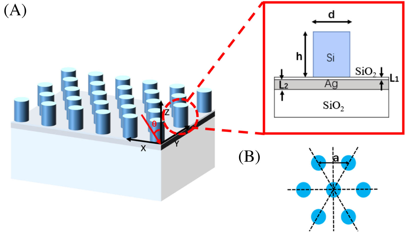
A schematic diagram of our metal–dielectric hybrid nanostructure is shown in Fig. 1. Si NPs with diameter and height are periodically arranged in a hexagonal lattice with a lattice constant . Such a Si NP array is placed on a multilayer substrate, wherein the thicknesses of the spacer and the Ag film are and , respectively. In the following simulations, we set , , , , and . The refractive indices of Ag and were taken in Ref. [26]. For the convenience of analysis, we have neglected the optical loss of Si (), and the dispersive and lossy case will be provided below in Fig. 9.
Figure 1.(A) Schematic illustration of the hybrid metal-dielectric nanostructure. It is composed of a Si NP array arranged in a hexagonal lattice, a thin spacer, an Ag film, and a substrate. The red arrow represents the direction of incident light. (B) Schematic of a unit cell of the Si NP array. In the following discussions, we choose , , , , and .
Figure 2(A) shows the simulated reflection spectrum of the considered hybrid structure under normal incidence of a plane wave. It is seen that two reflection dips exist at 596 and 746 nm. The corresponding electric field distributions in the plane are shown in Figs. 2(B) and 2(C). It is seen from Fig. 2(B) that the electric fields are strongly localized in the spacer between the Si nanorod and the Ag film, meaning that the reflection dip at 596 nm corresponds to an SPP resonance. On the other hand, the reflection dip at 746 nm is the result of a mirror image effect. The metal mirror image effect could transform the oscillating ED inside the dielectric nanoparticle into a magnetic polarization current [7,27,28], i.e., a mirror magnetic dipole (MMD), which can be verified from the field distribution in Fig. 2(C). Such an MMD in the considered nanostructure is the result of the original ED in the Si NP and its mirror electric dipole (MED), as illustrated in Fig. 2(D).
Figure 2.(A) Simulated reflection spectrum of the considered hybrid structure under normal incidence. The two reflection dips at 596 and 746 nm correspond to the SPP and MMD modes, respectively. Electric field distributions in the plane (B) at 596 nm and (C) at 746 nm. The arrows represent the electric field vectors. (D) Illustration of the MMD induced from the ED inside a nanoparticle and its mirror image in the metal film.
In order to investigate the optical effects induced by the SPP and MMD in the considered hybrid system, we simulated the reflection spectra as a function of incident angle for p- and s-polarizations, as shown in Figs. 3(A) and 3(B). The momentum-matching condition of the SPP modes inside the considered system can be written as where is the wave vector of the incident light, is the incident angle, and are the Bragg vectors associated with the two periodicities of the array, and and are integers indicating the orders of the scattering event. The wave vectors of the SPP modes can be calculated from where and are the relative pemittivities of metal and the surrounding medium. The calculated dispersion curve of the SPP mode is shown in Fig. 3(A). To illustrate the role of the Ag film in the hybrid structure, we also simulated the reflection spectra of the Si NPs with the same structural parameters placed on a substrate without the Ag film. The simulated results for p- and s-polarizations at different incidence angles are shown in Figs. 3(C) and 3(D), respectively.
Figure 3.Reflection spectra of the metal–dielectric hybrid system as a function of incident angle for (A) p- and (B) s-polarized plane waves. The SP-BICs and the accidental BICs are all highlighted by dashed circles. (C) and (D) are the polarized reflection spectra for the structure where Si NP array is placed on a thick substrate.
Two types of BICs are clearly seen in Fig. 3. The first one is the accidental BIC, as indicated by black dashed circles, whose formation mechanism will be discussed in detail later. At the same time, it can be noted that the remaining BICs are dark modes at normal incidence and become bright modes after changing the angle of incident light to break the symmetry. What is more, we find these BICs are located exactly at the high symmetry point (Γ point) through the energy band structure, which will be discussed in the following. The above typical features suggest that these BICs are SP-BICs [29].
As shown in Fig. 3(A), when the hybrid system is illuminated by p-polarized light, two SP-BICs appear at 554.5 and 628 nm in the case of normal incidence, and an accidental BIC exists at 750 nm at the incident angle of . For s-polarization, the SP-BIC at 554.5 nm still exists, while the other SP-BIC disappears, as shown in Fig. 3(B). The resonance mode at 628 nm results from the coupling of the SP-BIC with the SPP mode. When under s-polarized illumination, the SPP mode cannot be excited and the SPP-coupled SP-BIC no longer exists [22]. However, former research did not consider the effect of band degeneracy. Here, we discuss the polarization dependence of the SP-BIC in the proposed system based on group theory. By comparing Fig. 3(A) with Fig. 3(B), we can find that the SP-BIC at 741.5 nm (denoted by a white circle) only exists under s-polarized plane wave illumination. Similar phenomena are also observed in Figs. 3(C) and 3(D). From group theory, it can be surmised that some SP-BICs in a periodic array arranged in a hexagonal lattice are polarization-dependent when the structure satisfies symmetry. For a symmetric structure, doubly degenerate modes (i.e., doublets) and nondegenerate modes (i.e., singlets) exist in the -point, which may lead to the formation of four types of singlet BICs and one type of doublet BICs [30]. The singlet BICs are polarization-dependent while doublet BICs are not. The band structure of the Si NP periodically arranged in a hexagonal lattice for TM polarization is shown in Fig. 4. From Fig. 4, we can see that the SP-BIC at 755 nm [highlighted by a white circle in Fig. 3(D)] is a singlet BIC, and consequently, it only exists under s-polarization. The SP-BICs located at 550 and 585 nm [respectively highlighted by blue and green circles in Fig. 3(D)] are both doublet BICs, so they appear under both p- and s-polarizations. The BIC at 628 nm in Fig. 3(A), originated from the coupling of the polarization-independent doublet BIC at 585 nm in Fig. 3(D) and the SPP mode, becomes polarization-dependent because of the influence of the SPP mode. Therefore, the metal film can be used to manipulate the polarization dependence of the BICs in dielectric nanoparticles.
Figure 4.Simulated band structures for Si NPs deposited on a thick substrate without the Ag film under TM polarization. The structural parameters are the same as those in Fig. 1. Nondegenerate mode at 755 nm and doubly degenerate modes exist at 550 and 585 nm in the -point.
Since the SP-BICs cannot be directly observed under normal incidence [29], we use an obliquely incident light source with an incident angle of 3° to excite the quasi-BIC with similar properties. For comparison, in Figs. 5(A) and 5(B), we present the electric field distribution in the plane for the SPP-coupled quasi-BIC in the metal–dielectric hybrid structure and the quasi-BIC in an all-dielectric structure. It is seen that both quasi-BICs can lead to the enhancement of electric fields. Compared with the quasi-BIC in the dielectric structure, the SPP-coupled quasi-BIC exhibits a slightly weaker field enhancement because of the metal loss, but it still has a relatively large Q factor, as shown by the black curve in Fig. 5(C). It can be seen that the Q factor of the SPP-coupled quasi-BIC increases sharply as the incidence angle approaches , and a Q factor of is achieved at . In addition, it can be seen from Figs. 5(A) and 5(B) that the electric field of the quasi-BIC in the all-dielectric structure is mainly localized inside the Si NP, while the electric field corresponding to SPP-coupled quasi-BIC is confined in the spacer layer between the Si NP and the Ag film. To further demonstrate the advantages of our designed hybrid structure, we also calculated the Q factor and mode volume () of the plasmonic structure with Si NPs directly on top of the Ag layer without a spacer. We find that the Q value of the hybrid structure is slightly improved compared to the plasmonic structure (the Q factor is 142 and 126 at , respectively), as shown in Fig. 5(C). Furthermore, the mode volume of the hybrid structure is reduced by 1 order of magnitude as compared with the plasmonic structure, and the mode volume exhibits strong dependence on the gap width between the Si NP and the Ag film, as shown in Fig. 5(D).
Figure 5.Simulated electric field distributions in the plane for (A) the SPP-coupled quasi-BIC at 632.6 nm in our hybrid structure and (B) the quasi-BIC at 596.5 nm in the all-dielectric structure with an incident angle of 3°; (C) Q factor versus angle of incidence for the SPP-coupled quasi-BIC in hybrid structure (black) and plasmonic structure (red); (D) dependence of the optical mode volume ratio for the SPP-coupled quasi-BIC in hybrid structure (V) and plasmonic structure () on the thickness of the spacer.
Figure 6(A) shows the simulated reflection spectrum of the Si NP array placed on a substrate illuminated by a normal incidence plane wave. Here the structural parameters of the Si NPs are the same as those in Fig. 1(A). It is seen that two reflection peaks exist at 604 and 735.4 nm, respectively. The field distributions corresponding to the two reflection peaks are shown in Figs. 6(B) and 6(C). It can be clearly seen from Figs. 6(B) and 6(C) that an ED and an MD form at 604 and 735.4 nm, respectively. Such EDs and MDs, resulting from the Mie resonances in the Si NPs, lead to the strong reflection peaks shown in Fig. 6(A).
Figure 6.(A) Simulated reflection spectrum of the Si NP array placed on a substrate under normal incidence; field distributions corresponding to the reflection peaks (B) at 604 nm in the plane and (C) at 735.4 nm in the plane. The structural parameters of the Si NPs are the same as those in Fig. 1.
From Fig. 6(B), it is also seen that the direction of the ED in the Si NPs is along the direction, the same as that of the ED illustrated in Fig. 2(D). Consequently, the MMD in our hybrid structure is induced by the ED at 604 nm and its mirror image ED. The magnetic field (Hy) distributions in the plane corresponding to the MMD are shown in Fig. 7(A). Compared with the rightmost figure in Fig. 6(C), it can be seen that the MD in the Si NPs and the MMD in the hybrid structure point in opposite directions, which means that there is a phase shift between the MD and the MMD. In addition, the resonance wavelengths of the MD and the MMD are very close, and thus the two resonances can interfere destructively at a certain incident angle to form the accidental BIC, as shown in Fig. 3. To verify the above discussions, we simulated the electric field distributions corresponding to the accidental BIC at 750 nm, as shown in Fig. 7(B). The distributions for the intensity and vector of the electric field, corresponding to the two points B and A near the accidental BIC in Fig. 3(A), are also shown in Figs. 7(C) and 7(D), respectively. It can be seen from Figs. 7(C) and 7(D) that two different MDs (i.e., the MD in the Si NPs and the MMD in the hybrid structure) with opposite directions form near the accidental BIC. The destructive interference of these two MDs results in the formation of the accidental BIC at 750 nm, where the MD disappears, as shown in Fig. 7(B).
Figure 7.(A) Simulated magnetic field distributions corresponding to the MMD at 746 nm under normal incidence; (B) simulated electric field distributions corresponding to the accidental BIC in Fig. 3(A) appearing at 750 nm under the incident angle ; simulated electric field intensity and vector distributions corresponding to (C) point B in Fig. 3(A) at 748 nm under the incident angle and (D) point A at 752 nm under the incident angle .
To further demonstrate the contribution of the MD in Si NPs to the formation of accidental BICs, we investigate the reflection properties of the Ag NPs with the same size as the Si NPs in Fig. 1. Figure 8(A) shows the reflectance spectra of Ag NPs placed on air substrate, Ag substrate, and multilayer substrate under normal incidence; they are represented by black, red, and blue curves, respectively. It is seen that the Ag NP array does not excite the SPP or the MMD mode. When they are deposited on an Ag substrate, an MMD mode appears. Then, if the Ag substrate is replaced with the multilayer substrate (the structural parameters of the substrate are the same as those in Fig. 1), both SPP and MMD modes can be observed in the reflection spectrum. Figure 8(B) shows the reflection spectra of the Ag- hybrid structure at different incidence angles for p-polarization. Here, the dispersion curve of the SPP mode is calculated by Eqs. (1) and (2). It can be seen that the SPP-coupled SP-BIC still exists but the accidental BIC does not appear. The reason is that the Ag NPs can only excite the ED resonance, so that no MD can destructively interfere with the MMD to form the accidental BIC.
Figure 8.(A) Reflectance spectra under normal incidence for Ag nanopillars placed on air substrate, Ag substrate, and multilayer substrate, respectively; (B) reflection spectrum of Ag- multilayer structure as a function of incident angle for p-polarized plane wave. The sizes of the Ag NPs are the same as those of the Si NPs and the structural parameters of the multilayer substrate are the same as those of the substrate in Fig. 1.
In fact, Si in the visible range has losses. In order to explore the influence of these losses on our conclusion, we carried out the following research. We simulated the reflection spectra as a function of incident angle for p-polarization in a lossy case, as shown in Fig. 9(A); the refractive index of Si was taken in Ref. [26]. Comparing the results of Figs. 3(A) and 9(A), it can be found that the losses of Si only cause the redshift of the resonance wavelength. The Q value with losses is also calculated, as shown in Fig. 9(C); the Q values are only slightly reduced compared to the lossless case. In addition, mode volumes are almost the same for lossy and lossless cases, as shown in Fig. 9(D). Through the above analysis, it can be found that the influence of the losses on our conclusion is negligible.
Figure 9.(A) Reflection spectra of the metal–dielectric hybrid system as a function of incident angle for p-polarization plane waves in lossy case; (B) Q factor versus angle of incidence in a lossy case; (C) dependence of the optical mode volume ratio of lossless case (V) and lossy case () on the thickness of the spacer.
In conclusion, we have proposed a metal–dielectric hybrid nanostructure consisting of a Si NP array on a multilayer substrate and demonstrated that it supports both the SP-BICs and accidental BICs. We show that the SP-BIC can couple with the SPP, resulting in an order of magnitude reduction of mode volume and the strong field localization in the spacer between the Si NPs and the Ag film. Such a coupling effect also makes the original polarization-independent SP-BIC become polarization-dependent, which can be understood by group theory. In addition, we reveal that the accidental BICs in the considered hybrid structure result from the destructive interference between the MD inside the Si NPs and the MMD induced by the metal mirror effect. The existence or nonexistence of such accidental BICs depends on the presence or absence of the Ag film. Our findings offer an efficient platform to manipulate the light–matter interaction for potential applications such as lasing, sensing, and nonlinear devices.
[30] S. A. Dyakov, M. V. Stepikhova, A. A. Bogdanov, A. V. Novikov, D. V. Yurasov, Z. F. Krasilnik, S. G. Tikhodeev, N. A. Gippius. Photonic bound states in the continuum in Si structures with the self-assembled Ge nanoislands(2020).
Xuan Xiao, Yanxin Lu, Jiayi Jiang, Yihang Chen, "Manipulation of optical bound states in the continuum in a metal-dielectric hybrid nanostructure," Photonics Res. 10, 2526 (2022)