• High Power Laser Science and Engineering
  • Vol. 10, Issue 1, 010000e6 (2022)
M. Salvadori1、2、*, G. Di Giorgio1, M. Cipriani1, M. Scisciò1, C. Verona3, P. L. Andreoli1, G. Cristofari1, R. De Angelis1, M. Pillon1, N. E. Andreev4, P. Antici2, N. G. Borisenko5, D. Giulietti6、7, M. Migliorati8、9, O. Rosmej10、11, S. Zähter10、11, and F. Consoli1、*
Author Affiliations
  • 1Fusion and Nuclear Safety Department, ENEA, Frascati, Italy
  • 2INRS-EMT, Varennes, QC, Canada
  • 3Industrial Engineering Department, University of Rome “Tor Vergata”, Rome, Italy
  • 4Joint Institute for High Temperatures, RAS, Moscow, Russia
  • 5P. N. Lebedev Physical Institute, RAS, Moscow, Russia
  • 6Department of Physics, University of Pisa, Pisa, Italy
  • 7INFN of Pisa, Pisa, Italy
  • 8University of Rome “La Sapienza”, Rome, Italy
  • 9INFN of Rome, Rome, Italy
  • 10GSI Helmotzzentrum für Schwerionenforschung GmbH, Darmstadt, Germany
  • 11Goethe University Frankfurt, Frankfurt, Germany
  • show less
    DOI: 10.1017/hpl.2021.59 Cite this Article Set citation alerts
    M. Salvadori, G. Di Giorgio, M. Cipriani, M. Scisciò, C. Verona, P. L. Andreoli, G. Cristofari, R. De Angelis, M. Pillon, N. E. Andreev, P. Antici, N. G. Borisenko, D. Giulietti, M. Migliorati, O. Rosmej, S. Zähter, F. Consoli. Time-of-flight methodologies with large-area diamond detectors for ion characterization in laser-driven experiments[J]. High Power Laser Science and Engineering, 2022, 10(1): 010000e6 Copy Citation Text show less
    (a) A picture of the diamond surface taken with a Leica Wild M8 microscope equipped with the charge-coupled device camera JVC TK-C1480B. (b) A scheme of the diamond detector structure. The 150 μm polycrystalline diamond wafer is enclosed between two electrodes (made of 4 nm DLC, 4 nm Pt and 200 nm Au) providing a constant electric field allowing for charge collection.
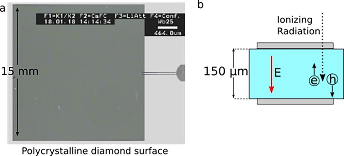
    Fig. 1. (a) A picture of the diamond surface taken with a Leica Wild M8 microscope equipped with the charge-coupled device camera JVC TK-C1480B. (b) A scheme of the diamond detector structure. The 150 μm polycrystalline diamond wafer is enclosed between two electrodes (made of 4 nm DLC, 4 nm Pt and 200 nm Au) providing a constant electric field allowing for charge collection.
    The typical signal provided by the polycrystalline diamond when exposed to single particles of 5.486 MeV. This was obtained by averaging over approximately 100 acquisitions and was used to retrieve the temporal response of the detector (4.1 ns).
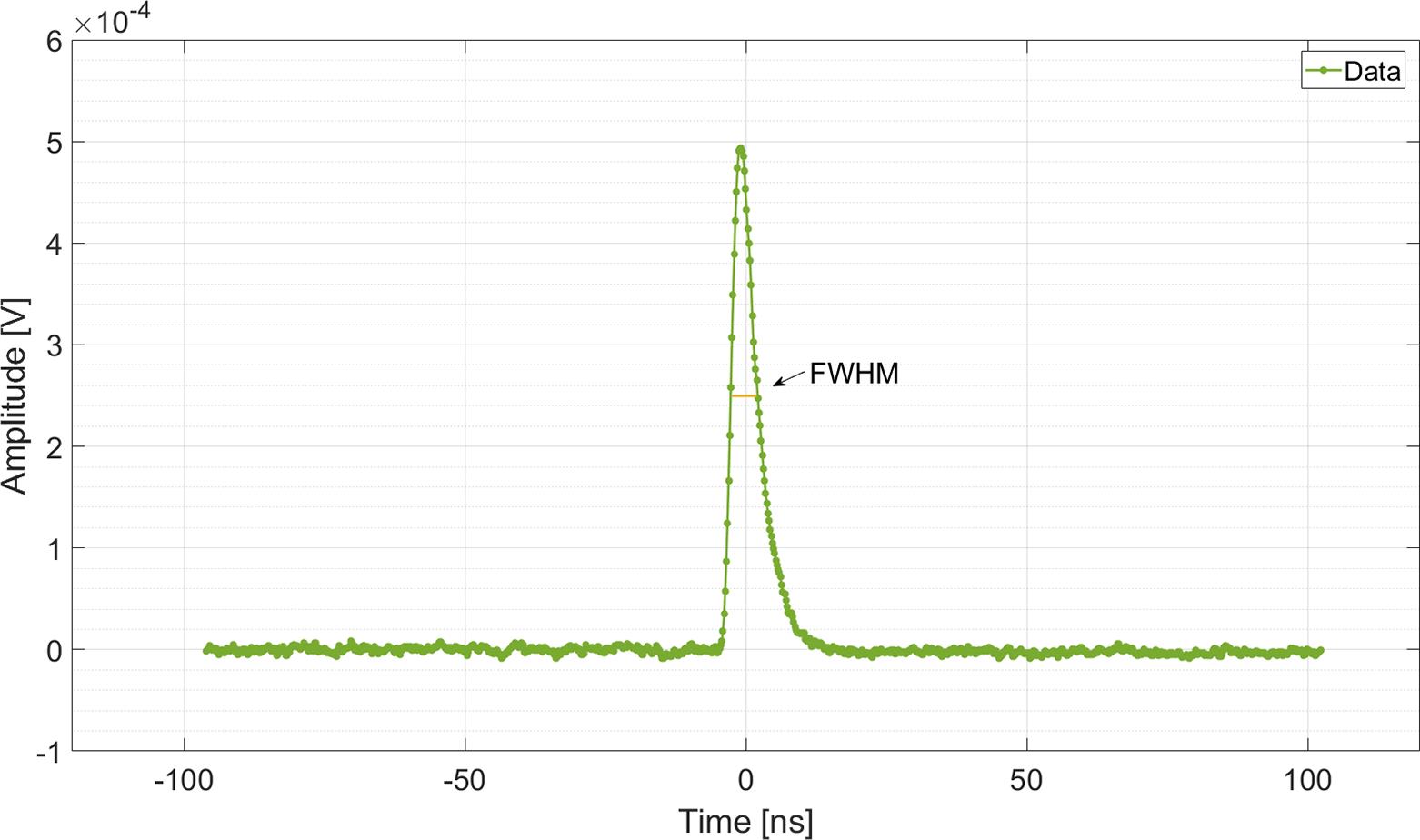
    Fig. 2. The typical signal provided by the polycrystalline diamond when exposed to single particles of 5.486 MeV. This was obtained by averaging over approximately 100 acquisitions and was used to retrieve the temporal response of the detector (4.1 ns).
    The pulse height spectrum obtained after 300 s of exposure to the 241Am radioactive sample. The estimated charge collection efficiency is approximately 42% ± 21%.
    Fig. 3. The pulse height spectrum obtained after 300 s of exposure to the 241Am radioactive sample. The estimated charge collection efficiency is approximately 42% ± 21%.
    The inner detector layout: (a) the diamond wafer mounted on a thin strip together with the electrical connection, where the bias to the electrodes is sent through an SMA connector; (b) the strip with the polycrystalline diamond detector is mounted on a support that allows its vertical alignment and is then fixed onto a stainless steel cap provided with SMA to BNC feedthroughs for vacuum.
    Fig. 4. The inner detector layout: (a) the diamond wafer mounted on a thin strip together with the electrical connection, where the bias to the electrodes is sent through an SMA connector; (b) the strip with the polycrystalline diamond detector is mounted on a support that allows its vertical alignment and is then fixed onto a stainless steel cap provided with SMA to BNC feedthroughs for vacuum.
    (a) The external case in which the support shown in Figure 4(b) is mounted. It is possible to see the inner Faraday cage and the two grids. (b) The scheme of the whole detector layout.
    Fig. 5. (a) The external case in which the support shown in Figure 4(b) is mounted. It is possible to see the inner Faraday cage and the two grids. (b) The scheme of the whole detector layout.
    The two copper grids placed in front of the diamond detector: (a) the polarized grid can be biased up to 5 kV and has a mesh with a 4.5 mm step; (b) the grounded grid is characterized by a denser mesh (2 mm step), which is suitable for effective closing of the inner Faraday cage.
    Fig. 6. The two copper grids placed in front of the diamond detector: (a) the polarized grid can be biased up to 5 kV and has a mesh with a 4.5 mm step; (b) the grounded grid is characterized by a denser mesh (2 mm step), which is suitable for effective closing of the inner Faraday cage.
    (a) The signal acquired by the D-Dot probe in the time domain. (b) The spectrum retrieved from the reported signal by suitable Fourier transform.
    Fig. 7. (a) The signal acquired by the D-Dot probe in the time domain. (b) The spectrum retrieved from the reported signal by suitable Fourier transform.
    The raw-time domain signal collected by the polycrystalline diamond detector during the described shot.
    Fig. 8. The raw-time domain signal collected by the polycrystalline diamond detector during the described shot.
    The proton spectrum obtained by the signal in Figure 8. The measured maximum proton energy is 2.6 ± 0.3 MeV. The black dashed line highlights the cutoff energy of the 20 μm aluminum filter.
    Fig. 9. The proton spectrum obtained by the signal in Figure 8. The measured maximum proton energy is 2.6 ± 0.3 MeV. The black dashed line highlights the cutoff energy of the 20 μm aluminum filter.
    The attenuation coefficient obtained by SRIM computation for the aluminum filter having nominal thickness of 20 μm.
    Fig. 10. The attenuation coefficient obtained by SRIM computation for the aluminum filter having nominal thickness of 20 μm.
    M. Salvadori, G. Di Giorgio, M. Cipriani, M. Scisciò, C. Verona, P. L. Andreoli, G. Cristofari, R. De Angelis, M. Pillon, N. E. Andreev, P. Antici, N. G. Borisenko, D. Giulietti, M. Migliorati, O. Rosmej, S. Zähter, F. Consoli. Time-of-flight methodologies with large-area diamond detectors for ion characterization in laser-driven experiments[J]. High Power Laser Science and Engineering, 2022, 10(1): 010000e6
    Download Citation