
M. Salvadori, G. Di Giorgio, M. Cipriani, M. Scisciò, C. Verona, P. L. Andreoli, G. Cristofari, R. De Angelis, M. Pillon, N. E. Andreev, P. Antici, N. G. Borisenko, D. Giulietti, M. Migliorati, O. Rosmej, S. Zähter, F. Consoli, "Time-of-flight methodologies with large-area diamond detectors for ion characterization in laser-driven experiments," High Power Laser Sci. Eng. 10, 010000e6 (2022)
- High Power Laser Science and Engineering
- Vol. 10, Issue 1, 010000e6 (2022)
Abstract
1 Introduction
Semiconductor detectors characterized by a wide band-gap, that is, silicon carbide and diamonds, are commonly used as time-resolved sensors for time-of-flight (TOF) measurements[1–8]. This technique is a valuable instrument for the real-time characterization of charged particles accelerated during laser–plasma interaction[9]. In particular, when coupled to semiconductor detectors, it allows one to retrieve the particle energy distribution with a good resolution (according to the temporal response of the detector, tolerances of the order of about 2% are achieved), and to reconstruct the associated spectra with high accuracy[8,10,11]. The latter can be retrieved by exploiting the working principle of semiconductor detectors. When ionizing radiation interacts with the bulk of the material, it releases its energy and produces a certain number of free electron–hole pairs, accordingly[12]. These charges are then collected at the electrodes generating the signal. Knowing the detector response and the ion type, it is possible to retrieve the number of particles impinging onto the detector for each energy range[8,13].
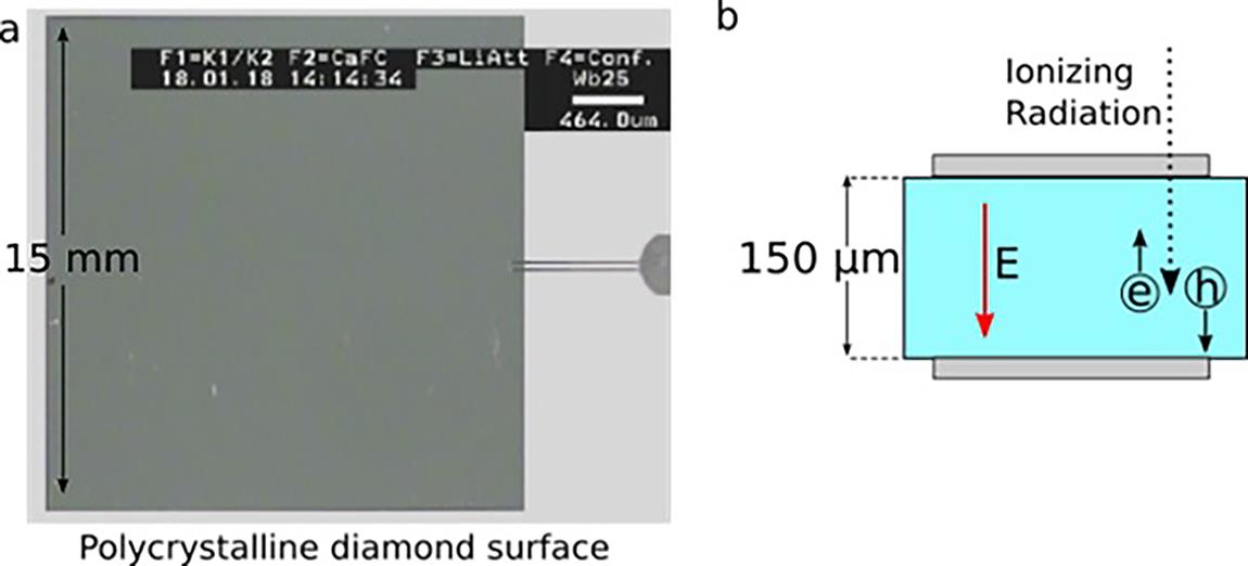
Figure 1.(a) A picture of the diamond surface taken with a Leica Wild M8 microscope equipped with the charge-coupled device camera JVC TK-C1480B. (b) A scheme of the diamond detector structure. The 150 μm polycrystalline diamond wafer is enclosed between two electrodes (made of 4 nm DLC, 4 nm Pt and 200 nm Au) providing a constant electric field allowing for charge collection.
The very high purity and crystalline quality of single crystal diamonds guarantee a considerably high value of charge carrier mobility and charge collection efficiency (CCE; up to 98%), resulting in TOF measurements characterized by a high temporal resolution (down to
When a high-intensity laser (>1016 W/cm2) interacts with matter, transient electromagnetic waves (spanning over hundreds of nanoseconds after the interaction) of remarkable intensity (up to the MV/m order) in the radiofrequency–microwave range are produced[16,17]. The presence of these strong electromagnetic pulses (EMPs) is a serious threat for electronic devices placed near the interaction point. Indeed, for classical TOF ion diagnostics, EMPs can couple both with the detection system and the acquisition system, often heavily hindering the effective measurement of accelerated ions[15]. To avoid this effect, an advanced TOF procedure has already been developed[8,15]. This offers a good rejection to the EMPs and allows for the suitable spectral representation of the detected protons. The employment of a large-area sensor significantly improves the detector sensitivity but, on the other hand, makes the detection system more prone to coupling with EMPs. Particular attention has been thus dedicated to the design of an advanced housing of the sensor, with the purpose of achieving high rejection to EMPs. This will allow it to be fruitfully employed even in the typical harsh environments of experiments that involve high-energy lasers interacting with matter, with the future purpose to successfully employ this type of detector in the new facilities under development around the world, such as Apollon in France (
Sign up for High Power Laser Science and Engineering TOC. Get the latest issue of High Power Laser Science and Engineering delivered right to you!Sign up now
In the following sections we will first introduce the basic concepts of the TOF technique coupled to semiconductor detectors. The novel detector design is then accurately described together with the performed characterization procedure. Finally, the results obtained during an experimental campaign, where remarkable levels of EMPs were produced, are presented and discussed.
2 Working principle
2.1 Time-of-flight technique and spectrum reconstruction
The TOF technique relies on the measurement of the time required by a particle for traveling over a known distance d
Actually, ion energies typically achieved in laser–plasma experiments are well below the relativistic limit; proton energies up to 10 MeV are routinely achievable with most laser systems, whereas only in the last years few tens of MeV have become more and more easily accessible, and the current record in terms of maximum proton energy is 94 MeV[19]. Thus, the previous relation simplifies to
Once the energy is known, from the amplitude of the signal, it is possible to obtain the number of particles impinging onto the detector by using the general relation[8,15]:
Here,
From the previous considerations it is therefore clear that for the spectrum estimation it is necessary to know the actual detector characteristics in terms of temporal response and CCE. For this purpose, the polycrystalline diamond was characterized by exposure to monochromatic
2.2 Time response and charge collection efficiency measurements
To appreciate the temporal response by single particle detection, the output of the diamond detector was connected to the biasing fast amplifier model Cividec (nominal gain G = 40 dB, bandwidth = 2 GHz) and to the LeCroy 620 Zi scope (bandwidth = 2 GHz, sample rate = 20 GS/s). The fast amplifier was necessary to both bias the detector and to increase the amplitude of the fast-varying signals to levels detectable by the scope.
The signal shown in Figure 2 has been obtained by averaging over several acquisitions performed with the detector biased at +250 V, typical bias used to feed the detector. The value of the applied voltage was chosen in order to use the sensor in the velocity saturation regime, that is, when the carrier velocity does not increase for a further increment of the suffered electric field[12].
![]()
Figure 2.The typical signal provided by the polycrystalline diamond when exposed to single  particles of 5.486 MeV. This was obtained by averaging over approximately 100 acquisitions and was used to retrieve the temporal response of the detector (4.1 ns).
From this kind of signal it is possible to retrieve the detector temporal response by estimating its full width at half maximum (FWHM), which resulted to be 4.1 ns.
The CCE was estimated by exposing the detector to the 241Am sample for 300 s. Thus, several events were detected by the diamond detector during the acquisition time. The output signals were processed by a conventional charge-sensitive electronic chain[12,13,20]. They were first integrated by a charge-sensitive preamplifier (ORTEC 142A). Then, the resulting voltage pulse was sent to a shaping amplifier (ORTEC 671) with gain and shaping time fixed to 200 and 6 μs, respectively. Finally, a multichannel analyzer connected to a computer sorted the input pulses in different bins according to their amplitude, given by the amount of collected charges, allowing one to obtain a pulse height spectrum (PHS). The spectrum acquired by the diamond detector is reported in Figure 3.
![]()
Figure 3.The pulse height spectrum obtained after 300 s of exposure to the 241Am radioactive sample. The estimated charge collection efficiency is approximately 42% ± 21%.
The 100% CCE bin corresponds to a collected charge equal to the number of charges ideally expected in the detector for a single incoming
Therefore, an ideal detector would produce a delta-like signal, peaked on the 100% bin, meaning that all the events produce the same amount of collected charge. Nevertheless, in the case of the polycrystalline diamond detector a broader spectrum is obtained with the peak shifted to lower values of CCE. This effect is due to several factors: trapping recombination centers, dislocations and grain boundary defects of polycrystalline diamond as well as fluctuations of the charge generation process, as reported in the literature[21–23].
The broadening of the spectrum means that even when detecting particles having the same energy that should generate the same number of charges inside the detector, the value of the collected charges varies. From the FWHM of the PHS it is therefore possible to infer the variability of the measured CCE. In this case a CCE value of approximately 42% with a tolerance of 21% was estimated.
In a previous work[13] the response of two typical single crystal diamond detectors presenting different electrodes layouts was characterized by using this methodology. The diamond with sandwich electrode configuration gave an almost ideal response with CCE (98 ± 2)%, whereas the interdigital electrodes layout showed a lower and broader CCE (68 ± 18)%.
2.3 Sensitivity enhancement estimation
The improved sensitivity of this detector with respect to the mentioned typical single crystal structures is due to the wider surface of the detector itself. This allows one to cover a larger solid angle, resulting in an overall greater sensitivity of the detection system.
In a TOF scheme, the sensitivity is given by the capability of the detector to supply a signal with intensity high enough to be effectively detected by the scope used for the measurement, according also to its noise floor.
A quality factor to express the actual sensitivity of the detector in schemes of laser–matter interaction could be defined as the product of CCE per detector area.
![]()
Figure 4.The inner detector layout: (a) the diamond wafer mounted on a thin strip together with the electrical connection, where the bias to the electrodes is sent through an SMA connector; (b) the strip with the polycrystalline diamond detector is mounted on a support that allows its vertical alignment and is then fixed onto a stainless steel cap provided with SMA to BNC feedthroughs for vacuum.
This relation allows for inferring the actual improvement in sensitivity of the polycrystalline by computing the ratio
As already mentioned, single crystal diamond detectors have higher CCE (68%–98%) but lower area (5 mm × 5 mm). According to data supplied in the previous section, the achieved sensitivity improvement by using the wide area polycrystalline diamond detector is in the range of 3.9–5.7, depending on the specific single crystal detector considered for the comparison.
2.4 EMP shielding
To be effectively employed in environments characterized by high levels of EMPs, the diamond sensor was mounted in a case optimized for optimal EMP rejection.
As shown in Figure 4(a), the diamond detector is located on a thin strip where all the electrical connections are built-in. In the developed detector design, these electrical connections are kept at a minimal length and are provided with an optimized grounding system and double-shielded cabling. The strip is then fixed on an ad hoc support that allows for its vertical alignment and mounting it onto a stainless steel cap (Figure 4(b)).
The whole assembly is then inserted into the final holder. This consists of two cylindrical structures, one containing the other. In Figures 5(a) and 5(b), it is possible to see that the assembly hosting the diamond detector fits into the inner cylinder that, when properly closed, works as a Faraday cage, providing an effective shielding to the detector from the external environment. The closure of the cage can be provided either with a thin metallic sheet or with a metallic grid designed with appropriate geometrical characteristics suitable for the shielding from the external electromagnetic waves.
![]()
Figure 5.(a) The external case in which the support shown in
![]()
Figure 6.The two copper grids placed in front of the diamond detector: (a) the polarized grid can be biased up to 5 kV and has a mesh with a 4.5 mm step; (b) the grounded grid is characterized by a denser mesh (2 mm step), which is suitable for effective closing of the inner Faraday cage.
Indeed, the detector holder is designed to allow the positioning of two grids mounted parallel to each other and to the diamond, as it is possible to see in Figures 5(a) and 5(b). Both the grids are made of copper and the diameter of the wires used for the mesh is 0.5 mm. The distance between the two grids and the distance between internal grid and diamond sensor are both of 40 mm. These values were due to mechanical and electrical reasons in the device development, to get reliable working operations. The first grid, shown in Figure 6(a), can be biased with voltages up to 5 kV through an internal cable with an MHV connector. The step of the mesh is 4.5 mm. This grid is isolated from the rest of the structure through a thermoplastic support made of white Delrin. The second internal grid, shown in Figure 6(b), is characterized by a denser wire mesh having a step of 2 mm. The grid material and geometrical parameters are chosen to be effectively used as closing components of the internal Faraday cage. Indeed, this grid is directly connected to the ground of the structure, and it is an integral part of the internal metallic shield, as can be seen in Figures 5(a) and 5(b).
We designed the grids by taking into account Ref. [24]. The internal grid (with 2 mm mesh step), meant for the actual electromagnetic shielding of the diamond, was designed to have transmission lower than 100 dB up to 10 GHz. This is the frequency range where EMP fields are known to be more intense[16]. The external grid, with a 4.5 mm mesh step, is also capable of giving good shielding, but it has been rather designed to have high particle transparency and yet to be robust for maintaining suitable biasing when required.
When the external grid is biased, the two-grid assembly provides a static electric field, which is useful to separate the electron contribution from the ionic component. As mentioned, the maximum biasing voltage is 5 kV, allowing electrons up to about 5 keV to be inhibited to reach the diamond. In this way ions with mass
The dimensions of the two squared grids are 18 mm × 18 mm (the external one) and 16 mm × 16 mm (the internal one). So, both are larger than the actual diamond. For particles having penetration ranges in Cu lower than the wire diameter, the employment of both of these grids would reduce the actual active surface of the diamond by a factor of approximately 25%, due to the area covered by the projection of the wires of the two grids on the diamond plane. Nevertheless, thanks to the large area of the polycrystalline diamond, this reduction does not remarkably affect the overall detector sensitivity and allows one to use the detector also without the necessity to use any further conductive shielding foil. However, the holder foresees the possibility to replace the inner grid with a thin foil filter right in front of the diamond detector, in order to cut the TOF contribution given by heavy ion detection, when necessary[8]. The combined action of the biased grid and the filter allows only protons to reach the detector, leading to an easier spectrum reconstruction.
All of these components are located in the external cylindrical case, made of stainless steel with walls having 2 mm thickness. These walls provide an additional shielding for electromagnetic waves with frequency down to approximately 500 Hz, exploiting the electromagnetic skin effect[25].
3 Experimental results
The performances of the described detector were successfully tested during an experimental campaign carried out at the PHELIX laser facility (GSI, Germany)[26,27]. During the experiment two laser pulses were combined to study the effect of controlled pre-plasma on laser-driven acceleration. A hydrodynamically stable, long scale-length near-critical density plasma was generated by irradiating low-density polymer foams with a nanosecond pulse kept at an intensity of approximately
This configuration, including the short and energetic laser pulse, is recognized to be one of the main scenarios where the produced EMP fields are most intense[16]. Thus, it represented a very good test to prove the EMP rejection of the developed detector assembly.
The EMP level was monitored by means of a custom D-Dot differential electric-field probe[16]. In Figure 7 the EMP spectrum for typical shot conditions is reported. It was acquired by a D-Dot probe placed behind a 10 cm thick Teflon shield at about 120 cm from the interaction point, where a cellulose triacetate (TAC, C12H16O8) cylindrical foam target (thickness = 425 μm, density 2 mg/cm3) fixed inside a Cu-washer of 2.5 mm in diameter[29] was irradiated with a first ns laser pulse followed, after 3 ns, by the 750 fs laser pulse having energy of 82.4 J (delivering on target 14.6 J). During this shot, the associated electric field estimated by the procedure reported in Ref. [30] exceeded the value of 100 kV/m. The signal covered the whole bandwidth of the scope used for the measurement (Lecroy 735 Zi, 3.5 GHz bandwidth)[31].
During a shot performed in similar conditions (for this shot the energy of the 750 fs laser pulse before compression was 86.1 J and the TAC foam thickness was 425 μm), the polycrystalline diamond detector provided the signal shown in Figure 8. The detector was biased at +300 V and placed on the horizontal plane at 90 cm from the interaction point at 37 degrees from the target normal axis. The signal provided by the diamond was collected by means of the Lecroy HDO 8108 scope (bandwidth = 1 GHz, effective number of bits (ENOB) = 8.6, sampling rate = 10 GS/s).
During this shot the diamond detector was covered with a 20 μm thick aluminum filter. This allowed to cut the heavier ion contribution at the expense of the loss of information in the lower energy region of the proton spectrum (below
The collected signal clearly presents a high signal-to-noise ratio, estimated to be 17.6 dB. The latter was inferred by comparing this signal with one acquired on a different channel of the same scope closed on a 50 Ω termination that allowed us to estimate the noise level due to the EMP coupling with the scope. The signal shown in Figure 8 was acquired with the channel scale set on 1 V/div, whereas the channel monitoring the noise level was set on 500 mV/div. In the signal, the temporal position of the photopeak is clearly recognizable as well as the instant when the protons with maximum energy are detected.
![]()
Figure 7.(a) The signal acquired by the D-Dot probe in the time domain. (b) The spectrum retrieved from the reported signal by suitable Fourier transform.
If necessary, to enhance the EMP shielding effectiveness while increasing the temporal resolution of the system, the TOF line can be extended by means of an aluminum pipe with a diameter of a few tens of mm mounted on a KF-40 flange on the chamber wall. This would enhance the effective shielding to the produced EMP thanks to the waveguide action performed by the pipe itself[25]. Indeed, a pipe having 40 mm provides a cut-off frequency of 4.39 GHz under which no electromagnetic wave can propagate[8,15,25]. Actually, as the pipe is not made of a perfect conductor, there is a steep exponential profile in the frequency domain for the attenuation toward frequencies lower than the cutoff. The same reason causes the electromagnetic waves having frequencies higher than the cutoff to be also attenuated according to the relation
![]()
Figure 8.The raw-time domain signal collected by the polycrystalline diamond detector during the described shot.
Here, ϵ and Ҽ are the electric permittivity and magnetic permeability of the medium filling the waveguide, respectively,
In Ref. [15] it was shown that without suitable care for EMP issues the diamond signal can be heavily affected by noise due to them, to the point where the photopeak is no more detectable and it is not possible to retrieve any spectra from the stored data. That campaign was performed at the FLAME facility (30 fs pulse, 3 J maximum energy and 5 × 10¹⁹ W/cm2 intensity on target), where a maximum value of 20 kV/m was achieved for typical EMPs produced. As reported in Ref. [16], for the FLAME regimes the produced EMPs are expected to be much lower than for the present PHELIX campaign. In fact, as previously mentioned in this manuscript, EMP values up to 100 kV/m were measured here, about five times higher than for the FLAME campaign. This gives the idea of the high quality of the typical signal shown in Figure 8 that was effectively obtained with the present detector.
The calibrated proton spectrum, shown in Figure 9 together with the associated tolerances, was then retrieved by following the procedure described in Ref. [8]. For this purpose the information on the detector temporal response and CCE obtained during the detector characterization was used, as shown in the previous section. Given the temporal resolution of the system
![]()
Figure 9.The proton spectrum obtained by the signal in
The maximum measured proton energy was 2.6 ± 0.3 MeV and, as usual, the number of detected protons decreases for increasing energy. The reason why the observed ion energies are relatively low if compared to the laser energy and intensity on the target has to be found in the main acceleration mechanism. This is not a classical target normal sheath acceleration (TNSA) but rather more a Coulomb explosion of the relativistic plasma channel, formed by the laser interacting with the long scale-length near-critical plasma[32]. Moreover, the main purpose of the experimental campaign was to study the enhancement in the electron acceleration exploiting the mechanism of direct laser acceleration[28]. The foam thickness was thus not optimized for ion acceleration, and this can explain the observed low energies. The same polycrystalline diamond detector has been recently used in a campaign performed at the VEGA 3 laser on TNSA ion acceleration and was capable of effectively detecting protons with energies up to a few tens of MeV[33]. A Thomson spectrometer was also mounted on a similar angle, and the maximum proton energy detected by the two diagnostics (TOF and Thomson) had a remarkable agreement[33]. So, the low maximum energy of the detected protons was physical, and not due to a limitation of the detector that can indeed sense much higher proton energies.
![]()
Figure 10.The attenuation coefficient obtained by SRIM computation for the aluminum filter having nominal thickness of 20 μm.
As already mentioned, the information for energies lower than 1.2 MeV was lost due to the presence of the 20 μm Al filter used for excluding the contribution of heavier ions, mounted in place of the inner grid. Nevertheless, the feature of the spectrum for higher energies was retrieved with high accuracy. These particles lost part of their energy on the Al foil, and to reconstruct their accurate spectrum it was necessary to make an estimation of the energy loss for each energy of the incoming particle. This was performed by means of SRIM [34] calculations, and the results for this attenuation are shown in Figure 10. The attenuation factor
4 Conclusions
In the last decades the field of laser–matter interaction underwent a rapid expansion. The growing availability of powerful laser systems paved the way for the application of laser-driven ion sources to different scenarios, from inertial confinement fusion to material analysis for security and cultural heritage[35–38]. This growth needs to be accompanied by the development of suitable diagnostic systems able to effectively characterize the interaction. To do this, it is crucial to face some challenges, for instance to work at a high repetition rate while maintaining a high sensitivity of the measurements, often hindered by the remarkable EMP fields typical of these scenarios.
In this work, we have described a novel detector design based on a 150 μm thick polycrystalline diamond sensor having a surface of 15 mm × 15 mm, characterized by a fast temporal response (FWHM = 4.1 ns) and a CCE of approximately 42%. This was employed in a TOF scheme during an experimental campaign held at the PHELIX laser facility at high pulse intensity and energy. This is recognized to be one of the main configurations where produced EMP fields are most intense[16] and in these conditions the detector assembly effectively proved its high EMP rejection. As a result, it was thus capable of providing high sensitivity together with a fast temporal response. According to Ref. [16], EMP levels scale with laser energy and mostly with laser intensities. The parameters used in the present campaign gave a significant number of generated EMPs, up to 100 kV/m at approximately 1 m distance from the target chamber center (TCC)[31]. Of course, EMPs up to the MV/m order can be expected at the same distance from the TCC for future experiments with laser intensities increased up to 1021 W/cm2 and beyond. Nevertheless, the present detector has demonstrated a very high rejection to the EMP fields and has the potential to supply high signal-to-noise ratios of the acquired signals and thus accurate real-time spectral characterization of ions in these extreme regimes.
The characteristics of this detector, in particular its high sensitivity, make it perfectly suitable to monitor processes characterized by low fluxes such as, for instance, the
References
[1] D. Margarone, L. Torrisi, S. Cavallaro, E. Milani, G. Verona-Rinati, M. Marinelli, C. Tuvè, L. Láska, J. Krása, M. Pfeifer, E. Krouský, J. Ullshmied, L. Ryć, A. Mangione, A. M. Mezzasalma. Radiat. Eff. Defects Solids, 163, 463(2008).
[2] D. Margarone, J. Krása, L. Giuffrida, A. Picciotto, L. Torrisi, T. Nowak, P. Musumeci, A. Velyhan, J. Prokůpek, L. Láska, T. Mocek, J. Ullschmied, B. Rus. J. Appl. Phys., 109, 103302(2011).
[3] G. Bertuccio, D. Puglisi, L. Torrisi, C. Lanzieri. Appl. Surf. Sci., 272, 128(2013).
[4] V. Scuderi, G. Milluzzo, D. Doria, A. Alejo, A. G. Amico, N. Booth, G. Cuttone, J. S. Green, S. Kar, G. Korn, G. Larosa, R. Leanza, P. Martin, P. McKenna, H. Padda, G. Petringa, J. Pipek, L. Romagnani, F. Romano, A. Russo, F. Schillaci, G. A. P. Cirrone, D. Margarone, M. Borghesi. Nucl. Instrum. Methods Phys. Res. Sect. A, 978, 164364(2020).
[5] M. Marinelli, E. Milani, G. Prestopino, C. Verona, G. Verona-Rinati, M. Cutroneo, L. Torrisi, D. Margarone, A. Velyhan, J. Krasa, E. Krousky. Appl. Surf. Sci., 272, 104(2013).
[6] R. D. Angelis, F. Consoli, C. Verona, G. D. Giorgio, P. Andreoli, G. Cristofari, M. Cipriani, F. Ingenito, M. Marinelli, G. Verona-Rinati. J. Instrum., 11, C12048(2016).
[7] M. Cipriani, F. Consoli, P. L. Andreoli, D. Batani, A. Bonasera, G. Boutoux, F. Burgy, G. Cristofari, R. D. Angelis, G. D. Giorgio, J. E. Ducret, A. Flamigni, D. Giulietti, K. Jakubowska, C. Verona, G. Verona-Rinati. J. Instrum., 14, C01027(2019).
[8] M. Salvadori, F. Consoli, C. Verona, M. Cipriani, M. P. Anania, P. L. Andreoli, P. Antici, F. Bisesto, G. Costa, G. Cristofari, R. De Angelis, G. Di Giorgio, M. Ferrario, M. Galletti, D. Giulietti, M. Migliorati, R. Pompili, A. Zigler. Sci. Rep., 11, 3071(2021).
[9] H. Daido, M. Nishiuchi, A. S. Pirozhkov. Rep. Prog. Phys., 75, 056401(2012).
[10] G. Milluzzo, V. Scuderi, A. Alejo, A. G. Amico, N. Booth, M. Borghesi, G. A. P. Cirrone, G. Cuttone, D. Doria, J. Green, S. Kar, G. Korn, G. Larosa, R. Leanza, D. Margarone, P. Martin, P. McKenna, G. Petringa, J. Pipek, L. Romagnani, F. Romano, A. Russo, F. Schillaci. Rev. Sci. Instrum., 90, 083303(2019).
[11] S. Vallières, M. Salvadori, P. Puyuelo-Valdes, S. Payeur, S. Fourmaux, F. Consoli, C. Verona, E. d’Humières, M. Chicoine, S. Roorda, F. Schiettekatte, P. Antici. Rev. Sci. Instrum., 91, 103303(2020).
[12] R. S. Sussmann. CVD Diamond for Electronic Devices and Sensors(2009).
[13] C. Verona, M. Marinelli, S. Palomba, G. Verona-Rinati, M. Salvadori, F. Consoli, M. Cipriani, P. Antici, M. Migliorati, F. Bisesto, R. Pompili. J. Instrum., 15, C09066(2020).
[14] F. Consoli, R. De Angelis, P. Andreoli, A. Bonasera, M. Cipriani, G. Cristofari, G. Di Giorgio, D. Giulietti, M. Salvadori. Front. Phys., 8, 561492(2020).
[15] M. Salvadori, F. Consoli, C. Verona, M. Cipriani, P. L. Andreoli, G. Cristofari, R. D. Angelis, G. D. Giorgio, D. Giulietti, M. P. Anania, F. Bisesto, G. Costa, M. Ferrario, M. Galletti, R. Pompili, A. Zigler, P. Antici, M. Migliorati. J. Instrum., 15, C10002(2020).
[16] F. Consoli, V. T. Tikhonchuk, M. Bardon, P. Bradford, D. C. Carroll, J. Cikhardt, M. Cipriani, R. J. Clarke, T. E. Cowan, C. N. Danson, R. De Angelis, M. De Marco, J.-L. Dubois, B. Etchessahar, A. L. Garcia, D. I. Hillier, A. Honsa, W. Jiang, V. Kmetik, J. Krása, Y. Li, F. Lubrano, P. McKenna, J. Metzkes-Ng, A. Poyé, I. Prencipe, P. Ra̧czka, R. A. Smith, R. Vrana, N. C. Woolsey, E. Zemaityte, Y. Zhang, Z. Zhang, B. Zielbauer, D. Neely. High Power Laser Sci. Eng., 8, e22(2020).
[17] F. Consoli, P. L. Andreoli, M. Cipriani, G. Cristofari, R. De Angelis, G. Di Giorgio, L. Duvillaret, J. Krása, D. Neely, M. Salvadori, M. Scisciò, R. A. Smith, V. T. Tikhonchuk. Philos. Trans. Royal Soc. A Math. Phys. Eng. Sci., 379, 20200022(2021).
[18] E. Woryna, P. Parys, J. Wołowski, W. Mróz. Laser Particle Beams, 14, 293(1996).
[19] A. Higginson, R. J. Gray, M. King, R. J. Dance, S. D. R. Williamson, N. M. H. Butler, R. Wilson, R. Capdessus, C. Armstrong, J. S. Green, S. J. Hawkes, P. Martin, W. Q. Wei, S. R. Mirfayzi, X. H. Yuan, S. Kar, M. Borghesi, R. J. Clarke, D. Neely, P. McKenna. Nat. Commun., 9, 724(2018).
[20] J. Forneris, A. Lo Giudice, P. Olivero, F. Picollo, A. Re, M. Marinelli, F. Pompili, C. Verona, G. Verona Rinati, M. Benetti, D. Cannata, F. Di Pietrantonio. Europhys. Lett., 108, 18001(2014).
[21] P. J. Sellin, A. Lohstroh, A. W. Davies, A. Galbiati, J. Parkin, S. G. Wang, A. Simon. Nucl. Instrum. Methods Phys. Res. Sect. B, 260, 293(2007).
[22] S. G. Wang, Q. Zhang, S. F. Yoon, J. Ahn. Mater. Res. Bullet., 37, 1033(2002).
[23] M. Marinelli, E. Milani, A. Paoletti, A. Tucciarone, G. Verona Rinati, M. Angelone, M. Pillon. J. Appl. Phys., 89, 1430(2001).
[24] R. Gunnarsson, M. Backstrom2015 IEEE International Symposium on Electromagnetic Compatibility. and , in (), p. 479.(2015).
[25] N. Marcuvitz. Waveguide Handbook(1951).
[26] V. Bagnoud, B. Aurand, A. Blazevic, S. Borneis, C. Bruske, B. Ecker, U. Eisenbarth, J. Fils, A. Frank, E. Gaul, S. Goette, C. Haefner, T. Hahn, K. Harres, H.-M. Heuck, D. Hochhaus, D. H. H. Hoffmann, D. Javorková, H.-J. Kluge, T. Kuehl, S. Kunzer, M. Kreutz, T. Merz-Mantwill, P. Neumayer, E. Onkels, D. Reemts, O. Rosmej, M. Roth, T. Stoehlker, A. Tauschwitz, B. Zielbauer, D. Zimmer, K. Witte. Appl. Phys. B, 100, 137(2010).
[27] V. Bagnoud, F. Wagner. High Power Laser Sci. Eng., 4, e39(2016).
[28] O. N. Rosmej, M. Gyrdymov, M. M. Günther, N. E. Andreev, P. Tavana, P. Neumayer, S. Zähter, N. Zahn, V. S. Popov, N. G. Borisenko, A. Kantsyrev, A. Skobliakov, V. Panyushkin, A. Bogdanov, F. Consoli, X. F. Shen, A. Pukhov. Plasma Phys. Control Fusion., 62, 115024(2020).
[29] N. G. Borisenko, A. M. Khalenkov, V. Kmetik, J. Limpouch, Y. A. Merkuliev, V. G. Pimenov. Fusion Sci. Technol., 51, 655(2007).
[30] F. Consoli, R. De Angelis, T. S. Robinson, S. Giltrap, G. S. Hicks, E. J. Ditter, O. C. Ettlinger, Z. Najmudin, M. Notley, R. A. Smith. Sci. Rep., 9, 8551(2019).
[31] M. Scisciò, F. Consoli, M. Salvadori, N. Andreev, N. Borisenko, S. Zähter, O. Rosmej. High Power Laser Sci. Eng., 9, e64(2021).
[32] A. Pukhov, Z.-M. Sheng, J. Meyer-ter-Vehn. Phys. Plasmas, 6, 2847(1999).
[33] M. Salvadori, P. L. Andreoli, M. Cipriani, G. Cristofari, R. De Angelis, S. Malko, L. Volpe, J. A. Perez Hernandez, J. I. Alpinaniz, A. Morace, P. Antici, M. Migliorati, G. Di Giorgio, F. Consoli. , , , , , , , , , , , , , and , arXiv:2112.10674 ().(2021).
[34] J. F. Ziegler, M. D. Ziegler, J. P. Biersack. Nucl. Instrum. Methods Phys. Res. Sect. B, 268, 1818(2010).
[35] M. Barberio, S. Veltri, M. Scisciò, P. Antici. Sci. Rep., 7, 40415(2017).
[36] M. Passoni, F. M. Arioli, L. Cialfi, D. Dellasega, L. Fedeli, A. Formenti, A. C. Giovannelli, A. Maffini, F. Mirani, A. Pazzaglia, A. Tentori, D. Vavassori, M. Zavelani-Rossi, V. Russo. Plasma Phys. Control. Fusion, 62, 014022(2020).
[37] P. Puyuelo-Valdes, S. Vallières, M. Salvadori, S. Fourmaux, S. Payeur, J.-C. Kieffer, F. Hannachi, P. Antici. Sci. Rep., 11, 9998(2021).
[38] L. Giuffrida, F. Belloni, D. Margarone, G. Petringa, G. Milluzzo, V. Scuderi, A. Velyhan, M. Rosinski, A. Picciotto, M. Kucharik, J. Dostal, R. Dudzak, J. Krasa, V. Istokskaia, R. Catalano, S. Tudisco, C. Verona, K. Jungwirth, P. Bellutti, G. Korn, G. A. P. Cirrone. Phys. Rev. E, 101, 013204(2020).


Set citation alerts for the article
Please enter your email address

© Copyright 2018-2021 | Chinese Laser Press. All Rights Reserved 沪ICP备15018463号-20