
Antardipan Pal, Yong Zhang, Dennis D. Yau. Monolithic and single-functional-unit level integration of electronic and photonic elements: FET-LET hybrid 6T SRAM[J]. Photonics Research, 2021, 9(7): 1369
- Photonics Research
- Vol. 9, Issue 7, 1369 (2021)
Abstract
1. INTRODUCTION
For decades, the downscaling of complementary metal oxide semiconductor (CMOS) technology has followed Moore’s law in order to obtain both improved performance and lower power consumption. In the data-centric era, the CMOS scaling is focusing more on low voltages, cost-effective processes, and high performance to meet the requirements of high-end mobile applications. Besides new technologies that have been developed on improving the performance on a device level, the geometrical layout of the CMOS circuit has also been changed from planar to three-dimension by overcoming various integration issues, and furthermore the techniques that allow heterogeneous integration of different materials systems (e.g., Si, Ge, and III–V groups) have been developed [1]. However, these developments cannot address the fundamental limitations of the pure CMOS circuits, the resistive capacitive (RC) delay associated with metallic wires, and the dielectric gate delay associated with field-effect transistors (FETs). These delays ultimately limit the data speed and energy consumption.
In the meantime, it has been recognized that integrating electronic and photonic elements on the same chip can potentially transform computing architectures and enable more powerful computers. It is now possible to integrate a large number of electronic devices and photonic components on a single chip to perform logic, memory, and interconnect functions [2,3]. However, typically, the photonic components only play the roles of providing high-speed communications between different electronic subsystems [3,4], for instance, in a photonic dynamic random access memory (DRAM) [5], rather than any active roles in processing or modifying information like logic gates. Both key advantages and challenges of photonic circuits can be generally understood without resolving to detailed circuit designs [6]. Despite the obvious advantage of photonic devices in speed, there are three major challenges to integrate photonic and electronic devices more closely: size mismatch, energy data rate (EDR), and cascadability [6–8]. For example, although photoconductive devices can potentially offer advantages in switching speed [9] and switching energy [10], one major drawback of using such devices, such as light-effect transistors (LETs) [10,11], is the inconvenience of using the output of one LET-based logic gate to directly drive the next similar logic gate without going through relatively inefficient electrical to optical energy conversion.
To explore the advantages of photonic devices but avoid the cascading issue in computing applications [12], we propose a hybrid approach where in an electronic integrated circuit we seek to replace some FETs that only serve the roles of switching a circuit on and off, such as the access transistors in a 6T static-random-access-memory (SRAM) cell by LETs, and accordingly the metallic word lines by optical waveguides (OWGs). Additionally, this application alleviates the challenges of size mismatch and EDR ( is desirable for on-chip communication) [6,8], because it does not require using light to address photonic devices individually [12] but in a group simultaneously as in the operation of conventional SRAM [13,14].
Sign up for Photonics Research TOC. Get the latest issue of Photonics Research delivered right to you!Sign up now
One of the most crucial concerns in many ultralow-power applications is energy efficiency. SRAM being one of the most critical building blocks in almost all digital systems, its packing density, speed, and power consumption are all crucial performance metrics [15,16]. SRAMs are generally used as high-speed cache memories providing a direct interface with a CPU at high speeds which are not possible to attain by other memory circuits.
However, on-chip caches typically consume 25%–45% of the total energy of a chip [17,18]. Moreover, in modern high-performance large-density memory circuits, more than 40% of the total energy is consumed due to leakage currents [19]. Hence, high-speed and energy-efficient embedded memories are desirable for a modern electronic system. Various device and circuit techniques [20–24] have been proposed to improve the overall performance of the SRAM and reduce the leakage in SRAM structures, but none is related to photonics.
A conventional 6T SRAM cell, schematically shown in Fig. 1, consists of six FETs labeled as M1–M6. M1, M2 and M3, M4 form the cross-coupled inverter pairs (latches), and M5, M6 are the access devices that allow the data stored in the cell to be accessed and modified by charging and discharging the output nodes Q and and bit lines BL and during the read and write operations. The two access transistors play an extremely crucial role in determining the overall speed, power dissipation, and stability of the cell [13,25]. Additionally, the three p-FETs, encircled in red in Fig. 1, are the bit line conditioning devices whose roles are to pre-charge and equalize the bit line voltages before each read and write operation. Their switching speed and energy consumption are also critical to the performance of the SRAM [25,26]. Many approaches in both device and circuit levels have been explored to offer various incremental improvements in the SRAM performance, particularly in speed and energy consumption [23,27,28].
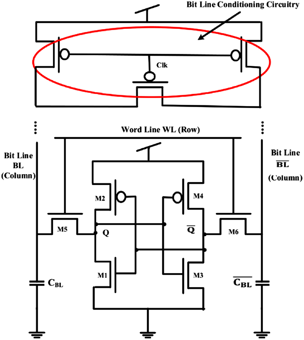
Figure 1.6T SRAM cell.
The proposed FET–LET hybrid 6T SRAM technology represents a drastically different approach that can offer major improvement on the read and write speeds and the corresponding energy consumptions after replacing the two access FETs with two LETs and accordingly the word line electrical wires with OWGs. This idea offers a more intimate integration of the electronics and photonics, namely on the single-functional-unit level. More importantly, this hybrid 6T SRAM is shown to offer drastic improvement of the SRAM performance in operation speed and thus total energy consumption over the conventional 6T SRAM. The focus of this work is on assessing the potential improvement of the 6T SRAM array itself, but the anticipated benefits of applying LETs in the peripheral circuits will also be discussed briefly.
2. ANALYSIS OF DELAYS AND ENERGY CONSUMPTIONS IN A CONVENTIONAL 6T SRAM ARRAY
The primary factors limiting the read and write speeds and the corresponding energy consumptions of a 6T SRAM array are the capacitances of the bit lines and word lines, and the characteristics of the access transistors.
A. Read and Write Delay Calculations
The critical capacitances of a 6T SRAM cell/array are calculated as follows [14,25]:
B. Read and Write Energy Calculations
Read and write energies are calculated as follows [25]:
C. Energy Consumption Associated with Leakage Currents
There are various types of leakage currents in a modern FET that contribute to the energy loss. They include subthreshold leakage current , gate leakage (gate-induced drain and source leakage currents, gate tunneling leakage currents through the bulk, source, and drain), and junction leakage currents (p-n junction leakage currents at the drain–substrate and source–substrate junctions) [33,34]. Although in the static state, the leakage currents of the two inverters may dominate the static energy consumption, during the write and read processes, the leakage of access transistors M5 and M6 also contributes to the total energy consumption. It can be roughly estimated that in a 6T cell about 40% of the total leakage is in the access paths of the cell [34].
3. ANALYSIS OF DELAYS AND ENERGY CONSUMPTIONS IN AN FET–LET HYBRID 6T SRAM
A. Light-Effect Transistor
An LET as shown in Fig. 2 is a semiconductor nanowire (NW) placed on an insulating substrate with two metal contacts at the ends [10]. The working mechanism of an LET is different from that of a traditional FET in that the source-drain conductivity of an LET is modulated by light or electromagnetic radiation of a suitable wavelength as in a photoconductive mechanism [10,35]. The advantage of an LET over an FET stems from various factors such as removal of physical gate, thus minimizing the complex gate fabrication process and random dopant fluctuations in FETs [36]. Hence, the LET can be scaled down to the quantum regime without the problem of short-channel effects (SCEs) that are common in nanoscale FETs [37]. Also, because the LET structure does not have a physical gate, the device speed is expected to be only limited by the carrier transit time or lifetime, whichever is smaller, rather than the capacitive delay as in the gated FET.
![]()
Figure 2.Schematic of a light-effect transistor (LET). (a) Output and (b) transfer characteristics of a prototype LET based on a CdSe nanowire.
Although the demonstrated prototype LETs were based on CdSe NWs [10], there is no limit to the material system per the device mechanism. At room temperature, many semiconductors (e.g., Si, SiC, InAs, InP, GaAs, CdSe) have saturation electron velocities in the range of – when the electrical field is of the order of 100 kV/cm [38,39], which implies a carrier transit time of the order of 1–0.1 ps for a 100 nm long NW. 100 nm is also the typical length scale of ballistic transport where the saturation velocity can be achieved. For longer NWs in the non-ballistic transport regime, the electron transit time depends on the electrical field. For Si at , electron velocity is around [38,39], and the carrier transit time () can be estimated to be 4.3 ps for a 300 nm long Si NW. If the NW in the LET can be scaled down to operate in the ballistic regime (), then ultrafast switching (of the order of 1 ps or faster) can be obtained. The ultrafast switching of the LET translates to ultrasmall switching energy. For instance, assuming a switching time (carrier transit time) (for a ballistic device), and an on-current of under , the electrical switching energy will be of the order of 1 aJ/switch.
However, in the LET, optical gating power also contributes to the switching energy. The net gating power required can be estimated by , where is the photon energy and is the photoconductive gain. Assuming , , to have , we get . Then, assuming , the optical switching energy will be , which leaves sufficient room allowing for below 100% light power delivery efficiency. In an even more idealistic case, assuming a ballistic device with a quantum impedance of 12.9 kΩ [40], transit time of 0.1 ps, S-D current of 1 μA, and no voltage loss at the contacts, the electrical switching energy can be as low as at a very low of only 13 mV [10]. For a prototype device with its output and transfer characteristics shown in Fig. 2, a single CdSe NW LET of 5 μm length and 80 nm in diameter studied previously [10], under 532 nm illumination of 110 nW (only about 6% of the power was actually absorbed), yielded at ; in dark, , which corresponds to about 1.5 pW static or off power. Estimating the switching energy for such a large device using the typical room temperature carrier lifetime in a II-VI semiconductor of the order of 100 ps, the total switching energy , which would still be better than typical FETs having switching energy of the order of 0.1–1 fJ/switch [41].
In FETs, the gate related RC delays predominate over the carrier transit-time delay; but in the LET, the carrier transit time through the NW channel is expected to be the predominant factor for determining the switching speed and energy of a discrete LET. Moreover, the ratio for an LET could be as high as [10], which is almost an order of magnitude better than that of advanced FETs. This reduces the leakage (leakage due to dark current) in the access paths and offers more flexibility in the 6T cell design with LET access devices.
B. Hybrid 6T SRAM with Access FETs Replaced by LETs
To take advantage of the high switching speed and low energy consumption of LETs, the two access transistors (M5 and M6) in the 6T cell of Fig. 1 are replaced by two LETs (L1 and L2) as shown in the prototype hybrid 6T cell of Fig. 3, where the word line is replaced by an OWG that transmits light to the LETs.
![]()
Figure 3.Prototype hybrid 6T SRAM cell with LET access.
To quantify the potential improvement, we consider a design with a moderate size LET based on a generic semiconductor NW: (length) and (diameter) and supported on an insulating substrate (e.g., ), as shown in Fig. 2. Also, a ballistic device with smaller dimensions ( and ) is considered, which yields a much reduced 6T cell and array area and high cell density.
For the LET structure, there will be no metal-semiconductor (MS)-junction capacitance that is equivalent to the drain or source capacitance (gate–drain or gate–source overlap capacitance along with the drain–substrate or source–substrate junction capacitance) of FETs, since there is neither a gate nor any electrical paths to ground between the MS structure and the substrate that has no electrical connection (only provides mechanical support) as opposed to the doped substrate of FETs. The photocurrents of NW photodetectors are typically in the range of 1–10 μA [42–44]. For the LET access device, the on-current is assumed to be 5 μA. The switching delay, as estimated by the transit time earlier, is assumed to be around 4 ps and 0.1 ps for the non-ballistic and ballistic cases, respectively.
C. Critical Capacitance, Read, Write Delay, and Energy Consumption of Hybrid 6T SRAM
The critical capacitances of the hybrid 6T SRAM with LET access devices are modified from the and calculated in Eqs. (1) and (3) as follows:
In Eq. (8), the modified bit line capacitance is predominantly the wire capacitance only, since the LET access devices do not have any MS junction capacitance as discussed previously. In Eq. (9), there are only the drain and gate capacitances of the core FETs. The drain equivalent capacitance of the access FET [ in Eq. (3)] is not present in the case of LET access devices due to the same reason. In the LET accessed SRAM, the word line capacitance () in Eq. (2) should be practically zero, since the access LETs neither have any gate capacitance, nor require a wired electrical signal to control the gates as in the case of access FETs, and the OWGs that route light do not contribute to any capacitance. Accordingly, the read and write delays and the corresponding energies in Eqs. (4)–(7) are modified as below, with and being replaced by and appropriate for the LET access devices, and all the and are replaced by and , keeping other parameters and values almost unchanged:
Analytical relations Eqs. (4)–(7) and Eqs. (10)–(13) are used to calculate a set of delay and energy consumptions for various 6T SRAM arrays (32 bytes−64 kB) with respectively, FET, LET, and ballistic LET access devices for direct comparison. Despite as approximations, these analytical relations offer more transparent insight to the underlying device physics than numerical simulations. To ensure their ability to yield results of acceptable accuracy for the purpose of comparing two vastly different technologies, the analytical relations, Eqs. (4)–(7), were first used to calculate read and write delays for the conventional 6T SRAM following simulation conditions used in literature [45], which could reproduce the simulation results with 26% average accuracy [45].
![]()
Figure 4.Read and write delay and energy for various SRAM arrays with FET, LET, and ballistic LET access devices. (a) Read delay, (b) read energy, (c) write delay, (d) write energy. The curves with LETs and ballistic LETs are indistinguishable.
On read delay, Fig. 4(a) reveals approximately a factor of 4 average reduction with LET access devices over FET access devices. Accordingly, on read energy, Fig. 4(b) reflects approximately a factor of 18 average reduction. On write delay, the average reduction shown in Fig. 4(c) is approximately a factor of 2, and on write energy, Fig. 4(d) shows approximately a factor of 4 average reduction. As summarized in Table 1, the results for both the read and write energies can indeed satisfy the requirement of EDR for on-chip photonic integration [6,8]. The general operating principle, mechanism, and conclusion are in principle applicable for LETs appropriately fabricated with any semiconductor.
4. DISCUSSION
A. Hybrid 6T Array without Peripherals
The improvement in the read delay of the hybrid 6T SRAM array is primarily due to the removal of the word line delay in Eq. (4) by the optical waveguide delay () in Eq. (10) that is almost negligible compared to the RC word line delay with FET access devices. The improvement in the write delay is due to the removal of the related term and the reduction of the overall bit line capacitance from to . Relatively, the improvement in the write delay is less than in the read delay, because the first term in the write delay in Eq. (5) takes the larger one of the two contributions, and hence the advantage of replacing the word line term in Eq. (11) by does not affect the overall write delay as much as it affects the read delay. Also, the highest reduction achieved in the read energy is mainly due to the replacement of the RC word line energy consumption in Eq. (6) (the first term) with FET access devices by a much smaller optical gating term in Eq. (12) (the first term) with LET access devices. Similarly, the improvement in the write energy in Eq. (13) is less than in the read energy in Eq. (12), due to the presence of the second and third terms in Eq. (13) where , and thus in Eq. (13) in Eq. (12), which to some extent lessens the amount of improvement in the write energy compared to the read energy.
Note that in the above analyses, the hybrid 6T SRAM array offers improved performance even with a smaller drive current (by a factor of 5) than the conventional 6T SRAM array. Since much lesser current is needed in the 6T hybrid cell, the core FETs (the FETs in the inverter pairs) can be scaled down to lesser device widths (FET drive current is proportional to the device width), which may offer saving in area for the 6T cell and hence for the whole array. However, we would like to point out that if the on-current of the hybrid 6T SRAM is kept at the same level as the conventional 6T SRAM, the read delay can be further reduced by approximately a factor of 5, but the improvement on write delay is less significant, because for a large 6T array it primarily depends on the .
The figure of merit of the SRAM array can be found from the energy–delay product (EDP) [25]. Considering 50% probability of the array being accessed in a cycle, and 50% probability for each of the read and write operations [25], it can be roughly estimated that the hybrid SRAM arrays (average EDP of the order of ) on an average exhibit more than 1 order of magnitude lower EDP than the regular SRAM arrays (average EDP of the order of ).
B. Possible Improvements in the Peripheral and Assist Circuits
Until now we have only focused on the effects of LET access devices on the 6T array and have not considered the potential benefits on the peripheral circuits [25,48] either as a direct consequence of replacing the access devices in the SRAM cells, or even further by replacing some FETs with LETs in the peripheral or assist circuits. First, replacing the FET access devices with the LETs in the 6T SRAM, and thus replacing the electrical word lines with OWGs, abolishes the need of the word line drivers, which not only reduces the capacitance and the RC-electrical energy consumption of the word line to practically zero, but may also reduce the capacitance and energy consumption of the column decoder circuitry [25]. It can be roughly estimated that over various array sizes, the hybrid array on average has almost 2 and 3 orders of magnitude lower word line delay and energy consumption, respectively, than the regular array with word line drivers [25]. A prototype 6T array with LET access devices and OWGs, keeping the core FETs and other peripherals almost unchanged, is shown in Fig. 5. The electrical row decoder circuit in a conventional SRAM array has to be replaced by an opto-electronic counterpart to illuminate the OWGs by appropriate optical sources, for example, nanoscale lasers [8].
![]()
Figure 5.Prototype hybrid 6T array.
Second, besides using LETs as the access devices, there may be a scope to replace some FET-based switches in other peripherals and assisting circuitry of the 6T array by LETs, which will further reduce the relevant delay and energy consumption, and hence further improve the performance of the SRAM array. For instance, there may be a possibility to replace the three p-FETs of the bit line conditioning circuitry of Fig. 3 by LETs, which will further reduce the bit line capacitances and hence bit line related delays and energy consumptions, especially for large 6T arrays.
C. Improvement on Leakage Using LET Access Devices
For the LET structure, all the leakage mechanisms (currents) for the FET mentioned in Subsection 2.C are eliminated except for the subthreshold current that is equivalent to the dark current of the LET. Since generally doping is not required for the nanowire in the LET, it can have very low dark current (e.g., of an order of few pA) [10].
LETs have a different turn-on mechanism and no SCEs of the FETs as discussed previously [10] and hence hybrid SRAMs will have minimal subthreshold leakage in the access paths. Since LETs do not have a physical gate, there will be neither any gate-related nor any SCE-induced leakage [33,34] in the access paths, and thus the leakage power consumption in the hybrid SRAM will be much reduced. Also, LETs do not have any unwanted p-n junctions or leakage paths to ground, hence the hybrid SRAM will also have no junction leakage [33,34] in the access paths, and the overall leakage will be much reduced. It can be estimated that there will be an overall reduction of roughly 35% in the total leakage current in a single hybrid 6T cell [34], which will be more advantageous in the case of a hybrid 6T array having a large number of 6T cells.
D. Compatibility with Metal Oxide Semiconductor Field Effect Transistor (MOSFET) and Scalability
In a typical circuit layout, the word line spacing is about “2 poly pitches,” which is of the order of 200 nm for 22 nm technology node and 100 nm for 7 nm technology node [49,50], respectively. OWGs fabricated on an insulating substrate can achieve subwavelength lateral size with very low loss, for instance, a Si waveguide of 400 nm for light at 1.55 μm with only 2.8 dB/cm loss [51]. Since photonic properties are scalable with wavelength, for the LETs operating at visible wavelengths, the OWG dimension can be significantly reduced (e.g., to around 140 nm at 532 nm illumination). Further reduction is possible by using plasmonic–dielectric hybrid waveguides, although with somewhat higher loss [52].
Alternatively, to alleviate the size mismatch between the light wavelength and the electronic device, one may envision the possibility to adopt somewhat different circuit layouts in the hybrid SRAM, for instance, arranging the access LETs of multiple cells of the same word line together such that they can be optically addressed as a group. This scheme can not only use the optical energy more efficiently, but may also increase the spacing of the OWG openings needed into the electronic layer. Additionally, as we know, the primary reasons for going down to smaller technology nodes are not only for saving space but also for improving performance. For the situations where the latter goal is more important, one could simply allow for a larger waveguide spacing. The optical waveguides are typically designed for interconnection between the circuits. In the hybrid SRAM, the optical paths are substantially shorter for on-chip operation. Thus, the scalability to a few hundred or even over one thousand cells/WL is not expected to be an issue for the propagation loss. The minimum light power output required from the optical decoder can be estimated to be of the order of only 8.5 μW per OWG for 1600 cells/WL, considering a propagation loss of 2.8 dB/cm [51] and an overestimated OWG length of 1 mm, and using the optical gating power estimate given in Subsection 3.A (2.5 nW/LET), which leaves a large room for less efficient implementation.
Heterogeneous integration of Si electronics with electronic and photonic components/structures made from compound semiconductors and other dielectric materials has been reported extensively with CMOS-compatible process flows [52–54]. The necessary technologies have largely been demonstrated for different applications, for instance, in the hybrid InGaAs/SiGe 6T SRAM [55], photonic waveguide cavity on Si [56], and SiN waveguides monolithically integrated with Ge-on-insulator [57], which all can be readily transferred to the proposed new integration scheme.
5. CONCLUSION
LETs offer high-speed and low-energy opto-electronic switching, where the switching delay is limited by carrier transit time, which can be made extremely small by using the nanowire-based device, particularly in the ballistic transport mode. In contrast, in FETs, it is generally RC switching, and hence it is much less energy efficient due to high gate-related capacitances in FETs. The biggest advantage of replacing the FET access devices by LETs is that the gate, source, and drain related capacitance and electrical word line are no longer present, which removes the word line delay as well as energy consumption. From the above delay and energy calculations of the hybrid 6T SRAM using LET access transistors, it can be concluded that the new hybrid 6T SRAM array is much more energy efficient with lesser read and write delays than the all FET 6T cells and arrays. In addition, LETs are expected to have much lower leakage currents than conventional FETs, and thus the hybrid 6T cell and array will have much lower leakage power dissipation than those with FET access devices. The use of the optical waveguide-based word line architecture in the hybrid SRAM array abolishes the need of electrical word lines and also the word line drivers, which will drastically reduce the total word line capacitance, RC-delay, and energy consumption to almost negligible compared to that in the conventional SRAM array. Furthermore, LETs may find useful applications in other peripheral and assist circuits of the SRAM array like the bit line conditioning circuit for improvement in speed and energy consumption. The proposed hybrid SRAM architecture offers an example of hybrid electronic–photonic integrated circuit with both electronic and photonic devices playing active roles synergistically.
Acknowledgment
Acknowledgment. This work was partially supported by fund from Bissell Distinguished Professorship at UNC-Charlotte. We thank Drs. Qiuyi Ye, Kwok Ng, and Amrutur Bharadwaj for valuable discussions and suggestions.
References
[1] H. H. Radamson, H. Zhu, Z. Wu, X. He, H. Lin, J. Liu, J. Xiang, Z. Kong, W. Xiong, J. Li, H. Cui, J. Gao, H. Yang, Y. Du, B. Xu, B. Li, X. Zhao, J. Yu, Y. Dang, G. Wang. State of the art and future perspectives in advanced CMOS technology. Nanomaterials, 10, 1555(2020).
[2] C. Sun, M. T. Wade, Y. Lee, J. S. Orcutt, L. Alloatti, M. S. Georgas, A. S. Waterman, J. M. Shainline, R. R. Avizienis, S. Lin, B. R. Moss, R. Kumar, F. Pavanello, A. H. Atabaki, H. M. Cook, A. J. Ou, J. C. Leu, Y.-H. Chen, K. Asanović, R. J. Ram, M. V. Popović, V. M. Stojanović. Single-chip microprocessor that communicates directly using light. Nature, 528, 534-538(2015).
[3] M. Smit, K. Williams, J. van der Tol. Past, present, and future of InP-based photonic integration. APL Photonics, 4, 050901(2019).
[4] IEEE Electronics. Heterogeneous Integration Roadmap 2019 Edition(2019).
[5] C. Batten, A. Joshi, J. Orcutt, A. Khilo, B. Moss, C. Holzwarth, M. Popovic, H. Li, H. Smith, J. Hoyt, F. Kartner, R. Ram, V. Stojanovic, K. Asanovic. Building manycore processor-to-DRAM networks with monolithic silicon photonics. 16th IEEE Symposium on High Performance Interconnects, 21-30(2008).
[6] D. A. B. Miller. Optical interconnects to electronic chips. Appl. Opt., 49, F59-F70(2010).
[7] D. A. B. Miller. Are optical transistors the logical next step?. Nat. Photonics, 4, 3-5(2010).
[8] C.-Z. Ning. Semiconductor nanolasers and the size-energy-efficiency challenge: a review. Adv. Photonics, 1, 014002(2019).
[9] S. Y. Chou, M. Y. Liu. Nanoscale tera-hertz metal-semiconductor-metal photodetectors. IEEE J. Quantum Electron., 28, 2358-2368(1992).
[10] J. K. Marmon, S. C. Rai, K. Wang, W. Zhou, Y. Zhang. Light-effect transistor (LET) with multiple independent gating controls for optical logic gates and optical amplification. Front. Phys., 4, 8(2016).
[11] Y. Zhang, J. K. Marmon. Light-effect transistor (LET). U.S. patent(2017).
[12] Y. Zhang. Light effect transistors for high speed and low energy switching and beyond. J. Phys. Conf. Ser., 1537, 012004(2020).
[13] S.-M. Kang, Y. Leblebici. CMOS Digital Integrated Circuits(1996).
[14] D. Hodges, H. Jackson, R. Saleh. Analysis and Design of Digital Integrated Circuits(2004).
[15] S. Panda, N. M. Kumar, C. K. Sarkar. Power, delay and noise optimization of a SRAM cell using a different threshold voltages and high performance output noise reduction circuit. 4th International Conference on Computers and Devices for Communication (CODEC), 1-4(2009).
[16] A. Garg, T. T. Kim. SRAM array structures for energy efficiency enhancement. IEEE Trans. Circuits Syst. II, 60, 351-355(2013).
[17] S. Gu, E. H. Sha, Q. Zhuge, Y. Chen, J. Hu. A time, energy, and area efficient domain wall memory-based SPM for embedded systems. IEEE Trans. Computer-Aided Design Integr. Circuits Syst., 35, 2008-2017(2016).
[18] D. Chang, I. Lin, L. Yong. ROHOM: requirement-aware online hybrid on-chip memory management for multicore systems. IEEE Trans. Computer-Aided Design Integr. Circuits Syst., 36, 357-369(2017).
[19] F. Menichelli, M. Olivieri. Static minimization of total energy consumption in memory subsystem for scratchpad-based systems-on-chips. IEEE Trans. Very Large Scale Integr. (VLSI) Syst., 17, 161-171(2009).
[20] X. Zhang, D. Connelly, H. Takeuchi, M. Hytha, R. J. Mears, T. K. Liu. Comparison of SOI versus bulk FinFET technologies for 6T-SRAM voltage scaling at the 7-/8-nm node. IEEE Trans. Electron Devices, 64, 329-332(2017).
[21] S. Strangio, P. Palestri, D. Esseni, L. Selmi, F. Crupi. Analysis of TFET based 6T SRAM cells implemented with state of the art silicon nanowires. 44th European Solid State Device Research Conference (ESSDERC), 282-285(2014).
[22] Z. Jakšić, R. Canal. Enhancing 6T SRAM cell stability by back gate biasing techniques for 10 nm SOI FinFETs under process and environmental variations. 19th International Conference Mixed Design of Integrated Circuits and Systems (MIXDES), 103-108(2012).
[23] R. Sinha, P. Samanta. Analysis of stability and different speed boosting assist techniques towards the design and optimization of high speed SRAM cell. 19th International Symposium on VLSI Design and Test, 1-6(2015).
[24] D. Nagy, G. Indalecio, A. J. García-Loureiro, M. A. Elmessary, K. Kalna, N. Seoane. FinFET versus gate-all-around nanowire FET: performance, scaling, and variability. IEEE J. Electron Devices Soc., 6, 332-340(2018).
[25] A. Shafaei, H. Afzali-Kusha, M. Pedram. Minimizing the energy-delay product of SRAM arrays using a device-circuit-architecture co-optimization framework. 53rd ACM/EDAC/IEEE Design Automation Conference (DAC), 1-6(2016).
[26] R. J. Evans, P. D. Franzon. Energy consumption modeling and optimization for SRAM’s. IEEE J. Solid-State Circuits, 30, 571-579(1995).
[27] K. Ma, H. Liu, Y. Xiao, Y. Zhang, X. Li, S. K. Gupta, Y. Xie, V. Narayanan. Independently-controlled-gate FinFET 6T SRAM cell design for leakage current reduction and enhanced read access speed. IEEE Computer Society Annual Symposium on VLSI, 296-301(2014).
[28] R. M. Premavathi, Q. Tong, K. Choi, Y. Lee. A low power, high speed FinFET based 6T SRAM cell with enhanced write ability and read stability. International SoC Design Conference (ISOCC), 311-312(2016).
[29] H. Iwai. Roadmap for 22 nm and beyond (invited paper). Microelectron. Eng., 86, 1520-1528(2009).
[30] Semiconductor Industry Association. 2007 International Technology Roadmap for Semiconductors (ITRS): Interconnect(2007).
[31] D. M. H. Neil, H. E. Weste. CMOS VLSI Design A Circuit and Systems Perspective(2011).
[32] http://ptm.asu.edu/latest.html. http://ptm.asu.edu/latest.html
[33] A. Calimera, A. Macii, E. Macii, M. Poncino. Design techniques and architectures for low-leakage SRAMs. IEEE Trans. Circuits Syst. I, 59, 1992-2007(2012).
[34] P. K. Bikki, P. Karupannan. SRAM cell leakage control techniques for ultra low power application: a survey. Circuits Syst., 8, 23-52(2017).
[35] N. F. G. Mott, R. W. Gurney. Electronic Processes in Ionic Crystals(1948).
[36] T. Shinada, S. Okamoto, T. Kobayashi, I. Ohdomari. Enhancing semiconductor device performance using ordered dopant arrays. Nature, 437, 1128-1131(2005).
[37] H. P. Wong. Beyond the conventional transistor. IBM J. Res. Dev., 46, 133-168(2002).
[38] O. Madelung. Semiconductors: Data Handbook(2004).
[39] M. E. Levinstein, M. Shur, S. L. Rumyantsev. Handbook Series on Semiconductor Parameters(1996).
[40] R. Landauer. Spatial variation of currents and fields due to localized scatterers in metallic conduction. IBM J. Res. Dev., 1, 223-231(1957).
[41] Semiconductor Industry Association. 2013 International Technology Roadmap for Semiconductors (ITRS)(2013).
[42] K. Das, S. Samanta, P. Kumar, K. S. Narayan, A. K. Raychaudhuri. Fabrication of single Si nanowire metal–semiconductor–metal device for photodetection. IEEE Trans. Electron. Devices, 61, 1444-1450(2014).
[43] C. Soci, A. Zhang, X.-Y. Bao, H. Kim, Y. Lo, D. Wang. Nanowire photodetectors. J. Nanosci. Nanotechnol., 10, 1430-1449(2010).
[44] H. Zhang, A. V. Babichev, G. Jacopin, P. Lavenus, F. H. Julien, A. Y. Egorov, J. Zhang, T. Pauporté, M. Tchernycheva. Characterization and modeling of a ZnO nanowire ultraviolet photodetector with graphene transparent contact. J. Appl. Phys., 114, 234505(2013).
[45] A. N. Bhoj, N. K. Jha. Parasitics-aware design of symmetric and asymmetric gate-workfunction FinFET SRAMs. IEEE Trans. Very Large Scale Integr. (VLSI) Syst., 22, 548-561(2014).
[46] E. Sicard. Introducing 10-nm FinFET technology in Microwind(2017).
[47] R. W. Mann, B. H. Calhoun. New category of ultra-thin notchless 6T SRAM cell layout topologies for sub-22 nm. 12th International Symposium on Quality Electronic Design, 1-6(2011).
[48] M. Q. Do, M. Drazdziulis, P. Larsson-Edefors, L. Bengtsson. Parameterizable architecture-level SRAM power model using circuit-simulation backend for leakage calibration. 7th International Symposium on Quality Electronic Design (ISQED), 557-563(2006).
[49] B. Nikolić. EE241B: advanced digital circuits lecture 2–scaling trends(2020).
[50] W. C. Jeong, S. Maeda, H. J. Lee, K. W. Lee, T. J. Lee, D. W. Park, B. S. Kim, J. H. Do, T. Fukai, D. J. Kwon, K. J. Nam, W. J. Rim, M. S. Jang, H. T. Kim, Y. W. Lee, J. S. Park, E. C. Lee, D. W. Ha, C. H. Park, H. Cho, S. Jung, H. K. Kang. True 7 nm platform technology featuring smallest FinFET and smallest SRAM cell by EUV, special constructs and 3rd generation single diffusion break. IEEE Symposium on VLSI Technology, 59-60(2018).
[51] T. Tsuchizawa, K. Yamada, H. Fukuda, T. Watanabe, J. Takahashi, M. Takahashi, T. Shoji, E. Tamechika, S. Itabashi, H. Morita. Microphotonics devices based on silicon microfabrication technology. IEEE J. Sel. Top. Quantum Electron., 11, 232-240(2005).
[52] J. T. Kim, S. Park. The design and analysis of monolithic integration of CMOS-compatible plasmonic waveguides for on-chip electronic–photonic integrated circuits. J. Lightwave Technol., 31, 2974-2981(2013).
[53] T. Spuesens, J. Bauwelinck, P. Regreny, D. V. Thourhout. Realization of a compact optical interconnect on silicon by heterogeneous integration of III–V. IEEE Photonics Technol. Lett., 25, 1332-1335(2013).
[54] P. Shen, C.-T. Chen, C.-H. Chang, C.-Y. Chiu, S.-L. Li, C.-C. Chang, M.-L. Wu. Implementation of chip-level optical interconnect with laser and photodetector using SOI-based 3-D guided-wave path. IEEE Photonics J., 6, 2500310(2014).
[55] L. Czornomaz, V. Djara, V. Deshpande, E. O’Connor, M. Sousa, D. Caimi, K. Cheng, J. Fompeyrine. First demonstration of InGaAs/SiGe CMOS inverters and dense SRAM arrays on Si using selective epitaxy and standard FEOL processes. IEEE Symposium on VLSI Technology, 1-2(2016).
[56] M. Li, J. Ling, Y. He, U. A. Javid, S. Xue, Q. Lin. Lithium niobate photonic-crystal electro-optic modulator. Nat. Commun., 11, 4123(2020).
[57] W. Xiong, G. Wang, Y. Du, H. Lin, X. Zhao, J. Yu, Z. Kong, Y. Dong, H. Jiang, Y. Tao, J. Li, W. Wang, H. H. Radamson. Integration of silicon nitride waveguide in Ge-on-insulator substrates for monolithic solutions in optoelectronics. J. Mater. Sci. Mater. Electron., 32, 6133-6140(2021).

Set citation alerts for the article
Please enter your email address
© Copyright 2018-2021 | Chinese Laser Press. All Rights Reserved 沪ICP备15018463号-20