• Acta Photonica Sinica
  • Vol. 52, Issue 1, 0116001 (2023)
Anchen WANG1, Zhongmei HUANG1、4、*, Weiqi HUANG1、2、**, Qian ZHANG1, Chun LIU1, Zilin WANG2, Ke WANG2, and Shirong LIU3
Author Affiliations
  • 1Institute of Nanophotonic Physics,College of Materials and Metallurgy,Guizhou University,Guiyang 550025,China
  • 2College of Physics & Electronic Engineering,Hainan Normal University,Haikou 571158,China
  • 3State Key Laboratory of Environment Geochemistry,Institute of Geochemistry Chinese Academy of Sciences Guiyang550003,China
  • 4Key Laboratory of Micro and Nano Photonic Structures(Ministry of Education),State key Laboratory of Surface Physics,Fudan University,Shanghai 200433,China
  • show less
    DOI: 10.3788/gzxb20235201.0116001 Cite this Article
    Anchen WANG, Zhongmei HUANG, Weiqi HUANG, Qian ZHANG, Chun LIU, Zilin WANG, Ke WANG, Shirong LIU. Influence of Silicon Oxide Layer Thickness on Electronic State Structure and Optical Properties of Si/SiO2 Interface[J]. Acta Photonica Sinica, 2023, 52(1): 0116001 Copy Citation Text show less
    Energy band structure of block α-cristobalite
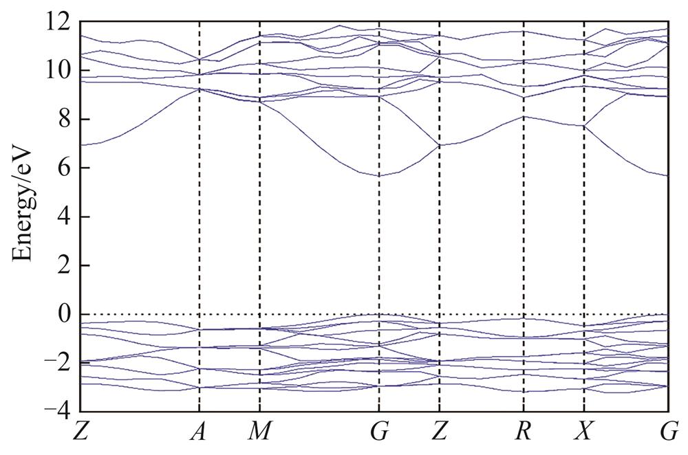
    Fig. 1. Energy band structure of block α-cristobalite
    Total density of states and partial electron density of bulk α-cristobalite
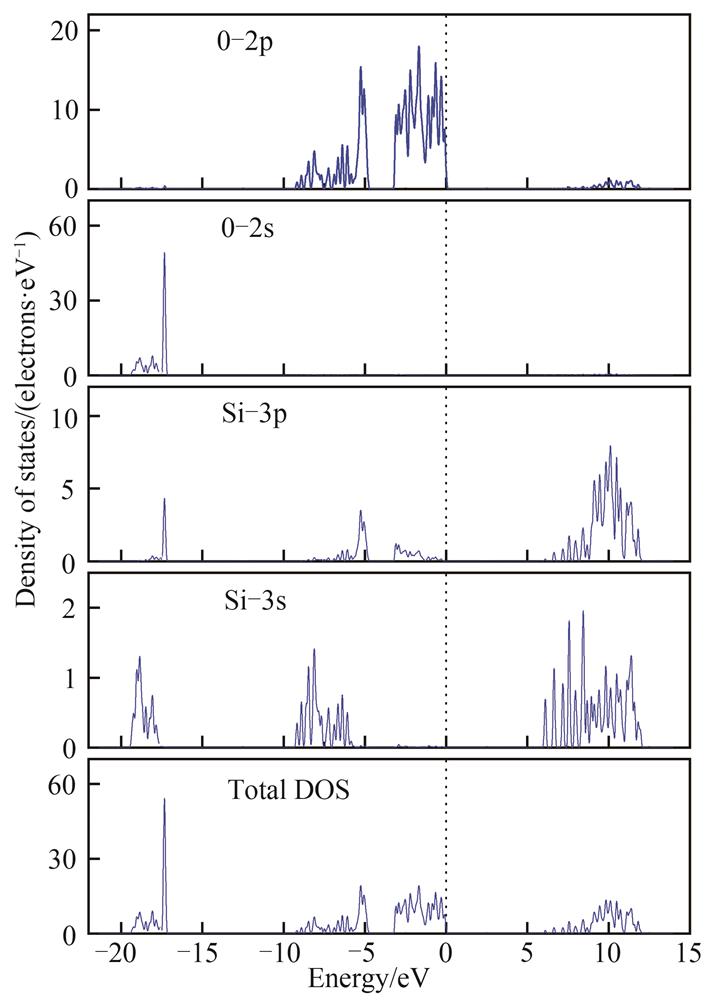
    Fig. 2. Total density of states and partial electron density of bulk α-cristobalite
    Structure of α-cristobalite film with different thickness.
    Fig. 3. Structure of α-cristobalite film with different thickness.
    Energy band structure of α-cristobalite film with different α-cristobalite thickness
    Fig. 4. Energy band structure of α-cristobalite film with different α-cristobalite thickness
    Relationship between the band gap of α-cristobalite and the thickness of α-cristobalite in thin films
    Fig. 5. Relationship between the band gap of α-cristobalite and the thickness of α-cristobalite in thin films
    Structure of Si/SiO2 interface with different thickness of silicon oxide layer
    Fig. 6. Structure of Si/SiO2 interface with different thickness of silicon oxide layer
    Energy band structure of Si/SiO2 interface with different thickness of silicon oxide layer
    Fig. 7. Energy band structure of Si/SiO2 interface with different thickness of silicon oxide layer
    Relationship between energy band gap of Si/SiO2 interface and thickness of silicon oxide layer
    Fig. 8. Relationship between energy band gap of Si/SiO2 interface and thickness of silicon oxide layer
    The total density of states and the density of partial wave electrons at the Si/SiO2 interface with the thickness of the silicon oxide layer of 1.047 nm and 2.887 nm
    Fig. 9. The total density of states and the density of partial wave electrons at the Si/SiO2 interface with the thickness of the silicon oxide layer of 1.047 nm and 2.887 nm
    Relationship between imaginary part of dielectric function of Si/SiO2 interface and thickness of silicon oxide layer
    Fig. 10. Relationship between imaginary part of dielectric function of Si/SiO2 interface and thickness of silicon oxide layer
    Relationship between absorption coefficient of Si/SiO2 interface and thickness of silicon oxide layer
    Fig. 11. Relationship between absorption coefficient of Si/SiO2 interface and thickness of silicon oxide layer
    Relationship between the refractive index of Si/SiO2 interface and the thickness of silicon oxide layer
    Fig. 12. Relationship between the refractive index of Si/SiO2 interface and the thickness of silicon oxide layer
    Optical microscope image of the prepared Si/SiO2 interface
    Fig. 13. Optical microscope image of the prepared Si/SiO2 interface
    PL spectrum on Si/SiO2 interface
    Fig. 14. PL spectrum on Si/SiO2 interface
    Anchen WANG, Zhongmei HUANG, Weiqi HUANG, Qian ZHANG, Chun LIU, Zilin WANG, Ke WANG, Shirong LIU. Influence of Silicon Oxide Layer Thickness on Electronic State Structure and Optical Properties of Si/SiO2 Interface[J]. Acta Photonica Sinica, 2023, 52(1): 0116001
    Download Citation