• Acta Photonica Sinica
  • Vol. 52, Issue 1, 0116001 (2023)
Anchen WANG1, Zhongmei HUANG1、4、*, Weiqi HUANG1、2、**, Qian ZHANG1, Chun LIU1, Zilin WANG2, Ke WANG2, and Shirong LIU3
Author Affiliations
  • 1Institute of Nanophotonic Physics,College of Materials and Metallurgy,Guizhou University,Guiyang 550025,China
  • 2College of Physics & Electronic Engineering,Hainan Normal University,Haikou 571158,China
  • 3State Key Laboratory of Environment Geochemistry,Institute of Geochemistry Chinese Academy of Sciences Guiyang550003,China
  • 4Key Laboratory of Micro and Nano Photonic Structures(Ministry of Education),State key Laboratory of Surface Physics,Fudan University,Shanghai 200433,China
  • show less
    DOI: 10.3788/gzxb20235201.0116001 Cite this Article
    Anchen WANG, Zhongmei HUANG, Weiqi HUANG, Qian ZHANG, Chun LIU, Zilin WANG, Ke WANG, Shirong LIU. Influence of Silicon Oxide Layer Thickness on Electronic State Structure and Optical Properties of Si/SiO2 Interface[J]. Acta Photonica Sinica, 2023, 52(1): 0116001 Copy Citation Text show less

    Abstract

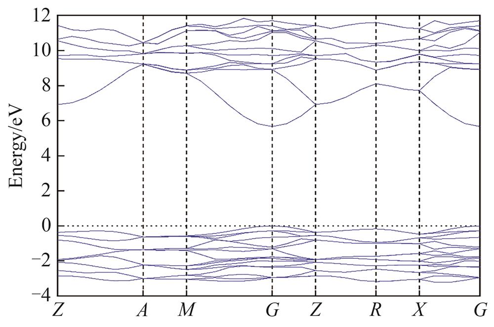
    The bulk α-cristobalite, the thin film α-cristobalite with different thicknesses and the Si/SiO2 interface with different silicon oxide layer thicknesses are all direct bandgap semiconductors. The thickness of the thin film α-cristobalite and the thickness of the silicon oxide layer at the Si/SiO2 interface gradually decrease, and the bottom of the conduction band moves continuously to the direction of the high energy level, and the energy band gap gradually increases, showing an obvious quantum confinement effect. The overlapping hybridization of the total density of states and the density of partial electronic states is weakened, and the valence band and conduction band of the energy band structure are more sparse. As the thickness of α-cristobalite decreases from 2.887 nm to 1.047 nm, the band gap of thin film α-cristobalite increases from 5.233 eV to 5.927 eV. As the thickness of silicon oxide decreases from 2.887 nm to 1.047 nm, the band gap of Si/SiO2 interface increases from 1.62 eV to 1.782 eV. With the decrease of the thickness of the silicon oxide layer at the Si/SiO2 interface, the quantum confinement effect is prominent and the energy band gap gradually increases. The bottom of the conduction band of the Si/SiO2 interface moves to the higher energy level with the decrease of the thickness of the silicon oxide layer. The electronic state structure change of the Si/SiO2 interface caused by the thickness change of the silicon oxide layer is similar to the electronic state structure change caused by the thickness change of the thin film α-cristobalite. The density of states and wavelength division states of Si/SiO2 interface with a thickness of 1.047 nm are all lower than those of Si/SiO2 interface with a thickness of 2.887 nm. As a result, the energy band gap is reduced, and the overlapping hybridization of electrons is weakened. The Si/SiO2 interface with a silicon oxide layer thickness of 1.047 nm has a very steep peak at -19.5 eV. It can be seen from the total density of states and partial wave electron density diagram of bulk α-cristobalite that this peak mainly comes from the contribution of 2s electrons of oxygen atoms in silicon oxide layer at Si/SiO2 interface, because the energy of 2s electrons of oxygen atoms in silicon oxide layer is higher than that of 3s electrons of silicon. Near fermi surface, the density of electronic states at Si/SiO2 interface mainly comes from the contribution of 2p states of oxygen atoms. The calculation results of optical properties show that the imaginary part of the dielectric function at the Si/SiO2 interface has a dielectric peak near 4.5 eV. With the decrease of the thickness of the silicon oxide layer at the Si/SiO2 interface, the dielectric peak slightly moves to the high energy direction, and the peak value of the dielectric peak keeps rising. This is caused by the decrease of the thickness of the silicon oxide layer in Si/SiO2 and the increase of the band gap of the Si/SiO2 interface. As the thickness of the silicon oxide layer decreases, the Si/SiO2 interface state density decreases near the left side of the Fermi plane, and the overlapping hybridization of electrons is weakened, so the energy consumed when the electric dipole is formed inside increases. There is an absorption peak at the Si/SiO2 interface near 6 eV, and the peak of the absorption peak of the absorption coefficient of the Si/SiO2 interface also increases significantly with the decrease of the thickness of the silicon oxide layer, and the peak position moves to the high energy direction, resulting in a blue shift . Therefore, the electronic state structure and optical properties of the Si/SiO2 interface can be effectively regulated by controlling the thickness of the Si oxide layer at the Si/SiO2 interface. In the experimental part, the nanosecond pulsed laser deposition method was used to prepare silicon oxide and its silicon thin film, and the oxygen-blowing annealing was performed at a high temperature of 1 000℃, and the growth thickness of the film was changed by controlling the annealing time. During PLD fabrication, a nanosecond pulsed Nd:YAG laser with a third-harmonic 355 nm laser beam was used to deposit silicon crystalline nanolayers on silicon oxide, thereby constructing edge electronic states. In the photoluminescence measurement, the edge electron state on the Si/SiO2 interface sample has a strong luminescence peak at 670 nm; under the excitation of 532 nm laser, the Si/SiO2 interface electrons can be excited from the valence band to the conduction band, and enter the edge electron state to form a strong quasi-excited light peak. The experimental result verifies the results of the energy band calculation: growing a silicon thin film on silicon oxide can form edge electronic states to effectively reduce its energy band gap and maintain its direct band gap characteristics. The electrons in the electronic state at the edge of Si/SiO2 interface can also be transported to the lower partial wave state, forming a luminescent band in the near infrared band. The detection results of the photoluminescence PL spectrum of the silicon crystalline thin film structure sample on silicon oxide verify the results of the computational study. The edge electronic states on the sample narrow the wide direct bandgap of silicon oxide to 1~2 eV, and the position of the luminescence peak is covering visible light and near-infrared bands, thus, the silicon-on-silicon thin film structure will have good application prospects in the fields of light-emitting and photovoltaics.
    Anchen WANG, Zhongmei HUANG, Weiqi HUANG, Qian ZHANG, Chun LIU, Zilin WANG, Ke WANG, Shirong LIU. Influence of Silicon Oxide Layer Thickness on Electronic State Structure and Optical Properties of Si/SiO2 Interface[J]. Acta Photonica Sinica, 2023, 52(1): 0116001
    Download Citation