• Acta Photonica Sinica
  • Vol. 51, Issue 8, 0851512 (2022)
Yao ZHAO, Linhan LIN*, and Hongbo SUN*
Author Affiliations
  • State Key Laboratory of Precision Measurement Technology and Instruments,Department of Precision Instrument,Tsinghua University,Beijing 100084,China
  • show less
    DOI: 10.3788/gzxb20225108.0851512 Cite this Article
    Yao ZHAO, Linhan LIN, Hongbo SUN. On-chip Optical Interconnection Based on Two-photon Polymerization(Invited)[J]. Acta Photonica Sinica, 2022, 51(8): 0851512 Copy Citation Text show less

    Abstract

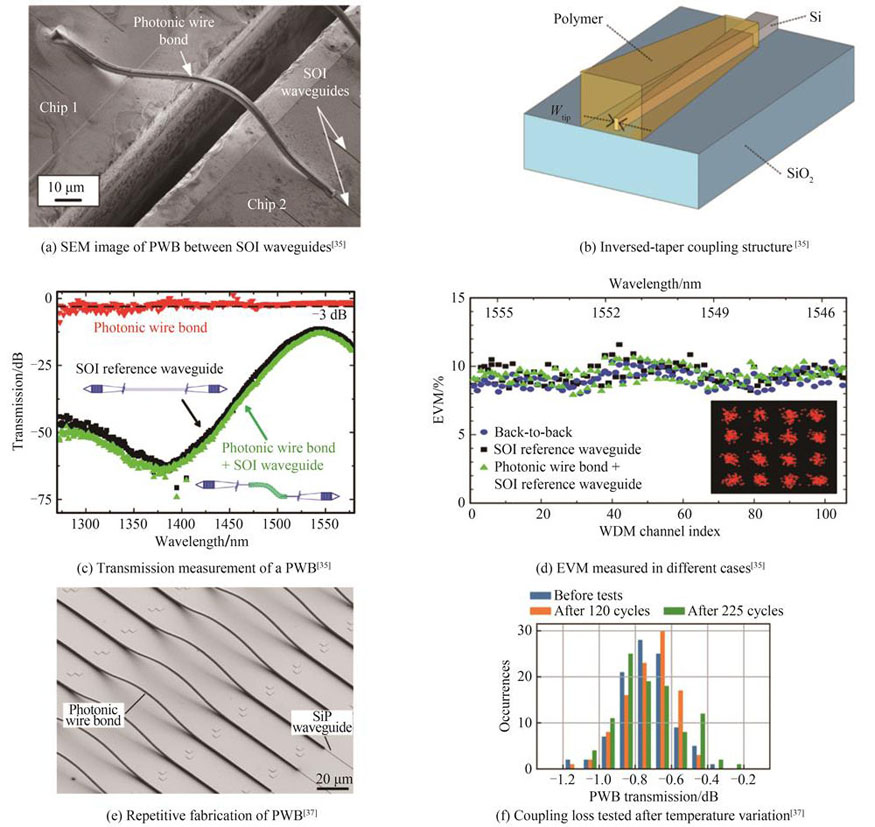
    Integrated photonic chip is a combination of optoelectronic devices such as laser light sources, low-loss waveguides, modulators, detectors, etc., to achieving specific functionality. Integrated photonic chip provides important applications in high-speed optical communication, quantum information processing, optical sensing, optical manipulation, and so on. However, the fabrication of optoelectronic devices relies on different materials, it is extremely difficult to achieve photonic integration. The traditional heterogeneous integration and monolithic integration methods cannot simultaneously solve the problems such as low positioning accuracy, low scalability, high loss, and low bandwidth. Inspired by the direct wire bonding of three-dimensional electrodeposition of metals and conductive polymer, a Direct Optical Wire (DOW) technique has been recently proposed. This technology utilizes the rapid volatilization of solvents in extruded polymer liquids to create arched polymer pathways for conducting light between single-mode fiber and gratings. However, the cross-section and path are not completely controllable and the accuracy is low, limiting the implementation of small interface and low transmission loss. Femtosecond laser has extremely high pulse power, which triggers the two-photon absorption at the focal point and cause crosslinking of the photoresist material. The two-photon absorption efficiency is proportional to the square of the light intensity, and the absorbed light intensity will rapidly decay with the distance from the focal point, so the resolution of Two-Photon Polymerization (TPP) can break the diffraction limit, with the lateral resolution below 100 nm. In addition, two-photon polymerization enables true three-dimensional, mask-free, and custom machining with high degrees of freedom, becoming an indispensable tool in the field of micro-nano additive manufacturing. In this paper, we review the field of laser additive manufacturing of on-chip optical components for photonic chip integration including Photonic Wire Bonding (PWB) and micro-space optical devices, and summarizes the development status of existing technologies, and the perspective of future development.PWB uses femtosecond laser for direct writing of polymer waveguides, leading to direct optical interconnection between different optical interfaces. During on-chip interconnect, the interface of the optical device, such as the refractive index distribution, spatial position, size, and orientation, are different from each other. PWB technology is able to solve the mismatching of multi-material optoelectronic devices in size, mold field and spatial layout. It allows connection of optical devices with low alignment accuracy (at the order of 10 μm), reducing the need of active alignment. Researchers used femtosecond laser to write polymer waveguide inside the SU8 photoresist to achieve on-chip optical interconnection between two SOI waveguides. To enable efficient coupling at the interface, they designed an inverted cone structure, reducing the coupling loss down to 1.6 dB. PWB was also applied on Si3N4 devices and optical connection between SOI waveguide and multi-core fiber. It exhibits good repeatability and thermal stability. In order to eliminate edge delamination caused by layer-by-layer scanning, spiral machining was carried out inside the structure to crosslink the structure, and a smooth shell was then written to reduce loss.Efficient coupling of Ⅲ/Ⅴ group light sources to silicon photonic circuits is one of the key challenges of integrated optics. PWB can also solve this key problem. The coupling between an InP based Horizontal Cavity Surface Emitting Laser (HCSEL) and a silicon photonic platform has been achieved. Due to the error in the tilt angle of the HCSEL deflector, the laser emission direction and the surface of the chip are not strictly vertical. Thus, the initial orientation of the PWB structure has to be adjusted accordingly. At the same time, in order to achieve mold field matching between the two interfaces, the shape of PWB has to be customized. For example, by processing the coupling gradient structure, the collection and deflection of the HCSEL laser can be achieved. Combining InP laser, silicon photonic modulators and Si waveguide, an eight-channel transmitter exhibits very good performance, offering an aggregate line rate of 448 Gbit/s.Different from the PWB technology, the technical scheme of the micro-space optical device does not involve the direct physical connection between two ports. However, through optical fabrication of micro-space optical device, such as micro reflectors, micro couplers, micro prisms, etc., the input space light or guided light signal can be processed, and then output in the form of space light or guided light. Micro-space optical device can realize the free conduction and characteristic transformation of optical signals, which is an important part of integrated optics. The concept of on-chip micro-space optical elements by TPP has long been proposed. A couple of optical devices, such as three-dimensional photonic crystals and phase-type Fresnel waveband sheets have been fabricated, while the latter achieves a diffraction efficiency of up to 68%. The fabrication of multilayer couplers, artificial compound eyes, and on-chip polarization rotators have also been demonstrated.With high precision and strong penetration, femtosecond laser is used as a tool to fabricate various three-dimensional polymer structures. Unique optical components are designed according to the characteristics of the optical chip, which is unattainable using traditional lithography technology. The highly freedom of femtosecond lasers greatly improve the alignment accuracy and enables mask-free machining. In the future, laser additive manufacturing will be applied to fabricate more complex microstructures based on more materials. Technical developments such as accurate image recognition and positioning in complex environments, wide horizontal and longitudinal range of processing, and reconfigurable fabrication, are expected to extend its application in three-dimensional optical chips.
    Yao ZHAO, Linhan LIN, Hongbo SUN. On-chip Optical Interconnection Based on Two-photon Polymerization(Invited)[J]. Acta Photonica Sinica, 2022, 51(8): 0851512
    Download Citation