• Chinese Journal of Lasers
  • Vol. 48, Issue 8, 0802005 (2021)
Yu Xiao1, Jinpeng Huo1, Tianming Sun1、2, Songling Xing1, Daozhi Shen1, Luchan Lin1、3, and Guisheng Zou1、*
Author Affiliations
  • 1Department of Mechanical Engineering, Tsinghua University, Beijing 100084, China
  • 2College of Materials Science and Engineering, Taiyuan University of Technology, Taiyuan, Shanxi 0 30024, China
  • 3Empa, Swiss Federal Laboratories for Materials Science and Technology, Dubendorf, Zurich 8600, Schweizerische Eidgenossenschaft
  • show less
    DOI: 10.3788/CJL202148.0802005 Cite this Article Set citation alerts
    Yu Xiao, Jinpeng Huo, Tianming Sun, Songling Xing, Daozhi Shen, Luchan Lin, Guisheng Zou. Nanojoining of p-Type Copper Oxide Nanowires Using Femtosecond Laser[J]. Chinese Journal of Lasers, 2021, 48(8): 0802005 Copy Citation Text show less
    Experimental flow of femtosecond laser connection CuO nanowires. (a) Dispersing CuO nanowires on PDMS; (b) target location selection under light mirror; (c) pressing down PDMS to substrate surface; (d) removal of nanowires by heating; (e) repeat (a)--(d) to form joint; (f) laser irradiation
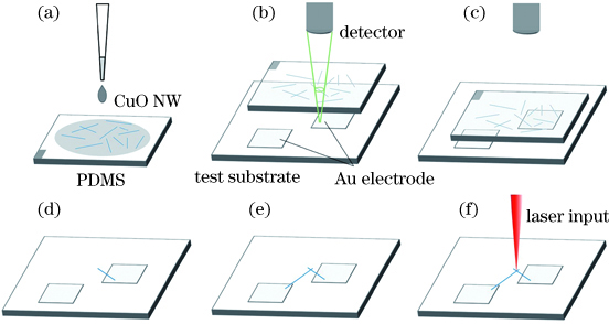
    Fig. 1. Experimental flow of femtosecond laser connection CuO nanowires. (a) Dispersing CuO nanowires on PDMS; (b) target location selection under light mirror; (c) pressing down PDMS to substrate surface; (d) removal of nanowires by heating; (e) repeat (a)--(d) to form joint; (f) laser irradiation
    Experimental apparatus for femtosecond laser fixed point nanojoining
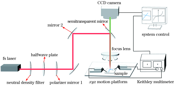
    Fig. 2. Experimental apparatus for femtosecond laser fixed point nanojoining
    Morphology of CuO nanowires. (a) CuO nanowires grown; (b) CuO nanowires on lower surface of PDMS, illustrated as dark field image; (c) TEM characterization results of CuO nanowires; (d) (111) plane of CuO
    Fig. 3. Morphology of CuO nanowires. (a) CuO nanowires grown; (b) CuO nanowires on lower surface of PDMS, illustrated as dark field image; (c) TEM characterization results of CuO nanowires; (d) (111) plane of CuO
    Nanojoining process and element distribution of CuO nanowires under femtosecond laser. (a) Untreated CuO nanowires; (b) distribution of copper elements on material surface; (c) distribution of oxygen elements on material surface; (d) CuO nanowires after connection; (e) damaged nanowires; (f) partially fractured nanowires
    Fig. 4. Nanojoining process and element distribution of CuO nanowires under femtosecond laser. (a) Untreated CuO nanowires; (b) distribution of copper elements on material surface; (c) distribution of oxygen elements on material surface; (d) CuO nanowires after connection; (e) damaged nanowires; (f) partially fractured nanowires
    Light field simulation results before and after CuO nanowire nanojoining. (a) Two CuO nanowires perpendicular to each other; (b) two CuO nanowires parallel to each other; (c) electric field intensity near contact point at different nanowire angles
    Fig. 5. Light field simulation results before and after CuO nanowire nanojoining. (a) Two CuO nanowires perpendicular to each other; (b) two CuO nanowires parallel to each other; (c) electric field intensity near contact point at different nanowire angles
    Electrical properties of single CuO nanowire. (a) Schematic of electrical measurement of single CuO nanowire; (b) electrical response range of CuO nanowires;(c) back-gate response of CuO nanowires; (d) back-gate response in logarithmic coordinates
    Fig. 6. Electrical properties of single CuO nanowire. (a) Schematic of electrical measurement of single CuO nanowire; (b) electrical response range of CuO nanowires;(c) back-gate response of CuO nanowires; (d) back-gate response in logarithmic coordinates
    Electrical properties of interconnection of CuO nanowires. (a) Schematic of electrical measurement of CuO nanowire interconnection; (b) interconnection enhancement curves of CuO nanowires under action of laser; (c) gradual damage curves of CuO nanowires subjected to laser; (d) regulation performance of nanowire gate after nanowire connection
    Fig. 7. Electrical properties of interconnection of CuO nanowires. (a) Schematic of electrical measurement of CuO nanowire interconnection; (b) interconnection enhancement curves of CuO nanowires under action of laser; (c) gradual damage curves of CuO nanowires subjected to laser; (d) regulation performance of nanowire gate after nanowire connection
    Performance curves of photodetector based on CuO nanowires. (a) Photoelectric response of single CuO nanowires under different light intensities and different voltages; (b) photoelectric response of single CuO nanowire with different light intensities over time; (c) comparison of device performance before and after laser nanojoining; (d) photoelectric response of device after laser nanojoining
    Fig. 8. Performance curves of photodetector based on CuO nanowires. (a) Photoelectric response of single CuO nanowires under different light intensities and different voltages; (b) photoelectric response of single CuO nanowire with different light intensities over time; (c) comparison of device performance before and after laser nanojoining; (d) photoelectric response of device after laser nanojoining
    Yu Xiao, Jinpeng Huo, Tianming Sun, Songling Xing, Daozhi Shen, Luchan Lin, Guisheng Zou. Nanojoining of p-Type Copper Oxide Nanowires Using Femtosecond Laser[J]. Chinese Journal of Lasers, 2021, 48(8): 0802005
    Download Citation