Objective With the rapid development of nanotechnology, new devices are gradually developing toward miniaturization, complexity, multimaterial, and multifunction. Selective nanojoining of nanowires is essential for the fabrication and assembly of high-performance functional nanounits. The development of good quality nanojoined structures based on new material systems has attracted considerable attention. Owing to its high peak power and small heat-affected zone, the femtosecond laser has unique advantages in accurate selective nanojoining. It is difficult to choose the parameters of laser processing joint fabrication, and material selection of nanowires, thus far, laser irradiation has only realized the nanojoining of metal-metal nanowires, metal-semiconductor nanowires, and n-n type semiconductor nanowires. The nanojoining system of nanowires under laser irradiation is still imperfect and needs further improvement. Therefore, we propose a method to successfully nanojoin two p-type copper oxide (CuO) nanowires using the local energy field of femtosecond laser with high spatial and temporal accuracy. Simultaneously, we investigate the influence of different femtosecond laser energy inputs on the interconnection joint and fabricate optoelectronic devices based on the nanojoined structure. The results show that the electrical response and photoelectric properties of the nanowire structure fabricated under femtosecond laser irradiation are significantly improved compared with those before nanojoining and can reach the level of the base material on electric properties.
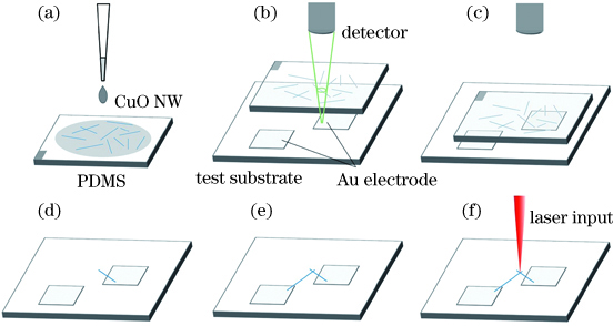
Methods The CuO joints are prepared using the dry transfer method. The nanowires are ultrasonically dispersed into an ethanol solution and spread on the surface of a polydimethylsiloxane(PDMS) film. The suitable target nanowires are obtained using an optical imaging system and aligned with the test electrode of the substrate using light transmittance of the film. The substrate is heated to 120 ℃ and held for 10--20 min to ensure that homogeneous joint of CuO nanowires is formed at the designated position on the substrate. (Fig.1(a)--(f)). The femtosecond laser is focused on the surface of the sample using a focusing microscope, and a CCD camera is used for real-time observation to ensure that the laser spot is focused accurately at the joint (Fig.1(g)). The continuous adjustment of laser power is achieved using a polarizer. The main characterization methods include a scanning electron microscope (SEM, Zeiss Supra 55), transmission electron microscope (TEM,JEM-2100F), and energy dispersive spectrometer (EDS). COMSOL Multiphysics 5.4 is used for simulation software, and Keithley 2636B is used for electrical tests.
Results and Discussions The prepared CuO nanowires are cylindrical with diameters ranging from 100--250 nm (Fig. 2). SEM is used to observe the morphology of CuO nanowire joints under different femtosecond laser parameters. When the single pulse energy density of the laser reaches 22.3 mJ/cm 2, the melting and wetting of the nanowires can be observed at the joint while the two base CuO nanowires remain intact, and almost no damage occurs, indicating that femtosecond laser can nanoweld two CuO nanowires with a minimal heat-affected zone (Fig.3(a)(d)). When the laser energy density is increased to 27 or 30 mJ/cm 2, a partial ablation or fracture of nanowires occurs, respectively, resulting in joint failure (Fig. 3 (e) and Fig. 3 (f)). The light field enhancement caused by geometric factors occurs at the contact area of nanowires by simulating the electric field distribution under laser irradiation using COMSOL, which is conducive to forming joints with a minimal heat-affected zone while nanojoining (Fig.4). The current response of the CuO homojunction device fabricated using this method is more than three orders of magnitude higher than that of the sample without nanojoining at 10 V bias, indicating that the properties of the nanowelded device are restored to the base material level (Fig. 5 and 6). CuO is a common optical sensing material. After femtosecond laser nanojoining, the fabricated CuO homojunction photoelectric sensor reaches the photoelectric performance of the base material, and the current growth ratio under 25.3 mW halogen lamp irradiation is the same as that of the base CuO nanowire (Fig.7).
Conclusions In this paper, we have successfully achieved the nanojoining between two p-type semiconductor CuO nanowires by combining the method of dry transfer and femtosecond laser irradiation. Under the influence of the laser energy field, the cylindrical CuO nanowires generate local energy field enhancement at the contact area due to the geometric factors, promoting the nanowelded joint formation with the minimal heat-affected zone. Under laser irradiation with a single pulse energy density of 22.3 mJ/cm 2, atomic-scale diffusion occurs at the joint of CuO nanowires to form a wetting structure, which transits the contact condition of nanowires from point contact to surface contact, greatly reduces the interface barrier, and widens the carrier transmission channel. This process increases the current level by more than three orders of magnitude compared with samples without nanojoining at 10 V bias, which almost reaches the current level of the base material. The photodetector based on the nanowelded structure obtains the same current growth ratio as that of the base material under a power of 25.3 mW of a halogen lamp. This study broadens the material system of semiconductor nanowires, which can be nanowelded, and provides a basis for the fabrication of miniaturized, high-performance, and multifunctional nanowire networks nanojoining.