
Zhanqiang Ren, Qingmin Li, Bo Li, Kechang Song. High wall-plug efficiency 808-nm laser diodes with a power up to 30.1 W[J]. Journal of Semiconductors, 2020, 41(3): 032901
- Journal of Semiconductors
- Vol. 41, Issue 3, 032901 (2020)
Abstract
1. Introduction
High power semiconductor lasers are extensively used in a variety of applications, such as solid-state laser and fiber laser pumping, material processing, as well as health care and military applications. Whilst tremendous improvements have been made over laser two decades or so, in terms of power level, efficiency, reliability etc., laser reliability remains a great challenge to both academic researcher and industrial R&D engineers[
The material of quantum-well active regions[
2. EPI and device design
The epitaxy material was grown using metal-organic chemical vapor deposition (MOCVD) and the structure contained an InGaAlAs single quantum well (SQW) sandwiched between the two separate confinement heterostructure (SCH) AlGaAs lasers. N-doping and p-doping were optimized such that lasers could produce the highest WPE. Our modelling showed that the internal optical loss was as low as 0.5 cm–1, and the WPE of 60.5% was achievable, when the operation current is 12 A. The length of chips is 2 mm long, and the aperture is 390 μm wide. The quantum well structure is shown in Table 1.
3. The fabrication of the semiconductor laser chip
The laser diode chip fabrication processes were implemented using standard optical lithography in combination with various etching techniques for lateral waveguide formation, and lift-off process for p-contact metal patterning. The deposition of n-contact metallization was carried out after substrate thinning. The wafer was cleaved into bars with a chip length of 2 mm and then the bars were coated with an anti-reflection (AR) film on the front facet and a high-reflection (HR) film on the rear facet with optimized facet coating process by electron beam evaporation, and the facet of laser was coated with AR of 0.5% and HR of 95% films. For the high COMD threshold and high reliability of the laser chips, special pretreatment and passivation of the crystal surfaces was carried out based on a plasma cleaning process on the front and rear facets. Finally, the laser bars were diced into chips and the chips were mounted p-side down on an AlN sub-mount with AuSn solder.
4. Power–current–voltage (P–I–V) characteristics and COMD measurement
4.1. P–I–V characteristics
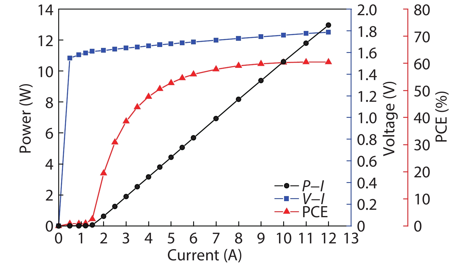
The fabricated laser diode was tested at 25 °C, and Fig. 1 shows the measured P–I–V curves, the dependence of power conversion efficiency on the injection current is shown as well. From the plot, one can see that the threshold is 1.5 A and the slope efficiency is 1.28 W/A. The maximum wall-plug efficiency is 60.5% when the current is 11 A. When the laser diode is used as a 10 W product, the operation current is 9.4 A, and the operation voltage is 1.76 V.
![]()
Figure 1.(Color online) A typical
4.2. Optical properties
Fig. 2 shows the measured spectrum of the fabricated laser devices. The spectrum was measured at 10 A in CW mode with the TEC temperature of 20 °C. Obviously, the center spectrum wavelength is 807.8 nm and spectrum width is only about 1.6 nm measured at the full-width at the half-maximum (FWHM). Fig. 3 plots the far field divergence angles for both slow and fast axes. The far field divergence angle was measured at 10 A, and the FWHM of the fast axis angle and the slow axis angle are of 32° and 6° respectively.
![]()
Figure 2.The spectrum of the fabricated laser diodes.
![]()
Figure 3.(Color online) The far field divergence angles of the fabricated laser diodes.
4.3. COMD measurement
Fig. 4 shows the P–I curve of COMD measurement under CW mode with the TEC setting temperature being 12 °C. From the figure, the maximum power of 30.1 W is obtained at the current of 29.5 A, after that point, the power begins to decrease because of the thermal rollover issue. It is important to note that at the maximum optical power, there is no observation of COMD happening, implying that the COMD threshold power is actually higher than the maximum power obtained in Fig. 4.
![]()
Figure 4.The COMD measurement.
5. Reliability test
In the reliability test, the accelerated aging condition was 12 A in CW mode and the cooling water temperature was 20 °C to evaluate the laser chip’s reliability performance. Fig. 5 shows the reliability test of the laser diodes. The five laser diode chips were randomly selected, by the time that this paper was submitted, the life test had reached 1000 h, and there was no failure during the test.
![]()
Figure 5.(Color online) Reliability test.
The definition of the life-time expectancy is the time taken when the output power decreased to 80% of the initial power level under fixed injection current. The average power degradation rate of the five chips is 1.61%/kh, based on this value, the life-time expectancy (LTE) can be calculated using the following equation:
where r is 1.61%/kh, the degradation rate per 1000 h, K is the accelerated factor which is about 5 for our test conditions, LTE is the life-time-expectancy. From Eq. (1), one can see the LTE to be around 62 111 h, which is longer than the marketing failure time 20 000 h.
6. Conclusion
By designed optimized laser structures as well as using improved facet pretreatment process, we have realized high WPE diode laser chip at 808 nm with 390 μm emitter width and 2 mm cavity length. The wall-plug efficiency of 60.5% was measured at 11 A, with the TEC setting temperature being 25 °C. The maximum output power of 30.1 W was achieved at 29.5 A, without occurrence of COMD, indicating our facet treatment process was truly robust. The reliability test shows that there is only very small decrease under in the laser power after 1000 h life-time test under 12 A accelerated aging condition, from which one can calculate that lifetime expectancy can be as long as 62 111 h.
Acknowledgment
This work was supported by the Natural Science Basic Research Plan in Shaanxi Province of China (No. 2018GY-005, No. 2017GY-065, No. 2017KJXX-72)
References
[1] W Gao, L Cheng, K J Luo. High power high reliable single emitter laser diodes at 808 nm. Proc SPIE, 6456, 64560B(2007).
[2] J Van de Casteele, M Bettiati, F Laruelle et al. High reliability level on single-mode 980 nm – 1060 nm diode lasers for telecommunication and industrial applications. Proc SPIE, 6876, 68760P(2008).
[3] Y K Sin, N Presser, B Foran et al. Investigation of catastrophic degradation in high power muliti-mode InGaAs strained quantum well single emitters. Proc SPIE, 6870, 68760R(2008).
[4] M Ziegler, J W Tomm, U Zeimer et al. Imaging catastrophic optical mirror damage in high-power diode lasers. J Electron Mater, 39, 709(2010).
[5] L Bao, J Wang, M DeVito et al. Reliability of high performance 9xx-nm single emitter diode lasers. Proc SPIE, 7583, 758302(2010).
[6] J Gilly, P Friedmann, H Kissel et al. High power broad area lasers optimized for fiber laser pumping. Proc SPIE, 8241, 82410T(2012).
[7] M Levy, N Rappaport, G Klumel et al. High-power single emitters for fiber laser pumping across 8xx nm – 9xx nm wavelength bands. Proc SPIE, 8241, 82410A(2012).
[8] Y K Sin, S LaLumondiere, B Foran et al. Catastrophic optical bulk damage (COBD) processes in aged and proton-irradiated high power InGaAs-AlGaAs strained quantum well lasers. Proc SPIE, 8605, 86050M(2013).
[9] S J Lee, H J An, T Ji. Optimization of high and anti-reflective facet coating for near infrared high power laser diode. Adv Sci Technol Lett, 139, 418(2016).
[10] B Leonhauser, H Kissel, A Unger et al. Feedback-induced catastrophic optical mirror damage (COMD) on 976 nm broad area single emitters with different AR reflectivity. Proc SPIE, 8965, 896506(2014).
[11] Y Sin, Z Lingley, M Brodie et al. Catastrophic optical bulk degradation (COBD) in high-power single- and multi-mode InGaAs–AlGaAs strained quantum well lasers. Proc SPIE, 10086, 100860S(2017).
[12] Y Zhang, Y Q Ning, L S Zhang et al. Design and comparison of GaAs, GaAsP and InGaAlAs quantum-well active regions for 808-nm VCSELs. Opt Express, 19, 12569(2011).

Set citation alerts for the article
Please enter your email address
© Copyright 2018-2021 | Chinese Laser Press. All Rights Reserved 沪ICP备15018463号-20