
Rongsheng Lu, Ang Wu, Tengda Zhang, Yonghong Wang. Review on Automated Optical (Visual) Inspection and Its Applications in Defect Detection[J]. Acta Optica Sinica, 2018, 38(8): 0815002
- Acta Optica Sinica
- Vol. 38, Issue 8, 0815002 (2018)
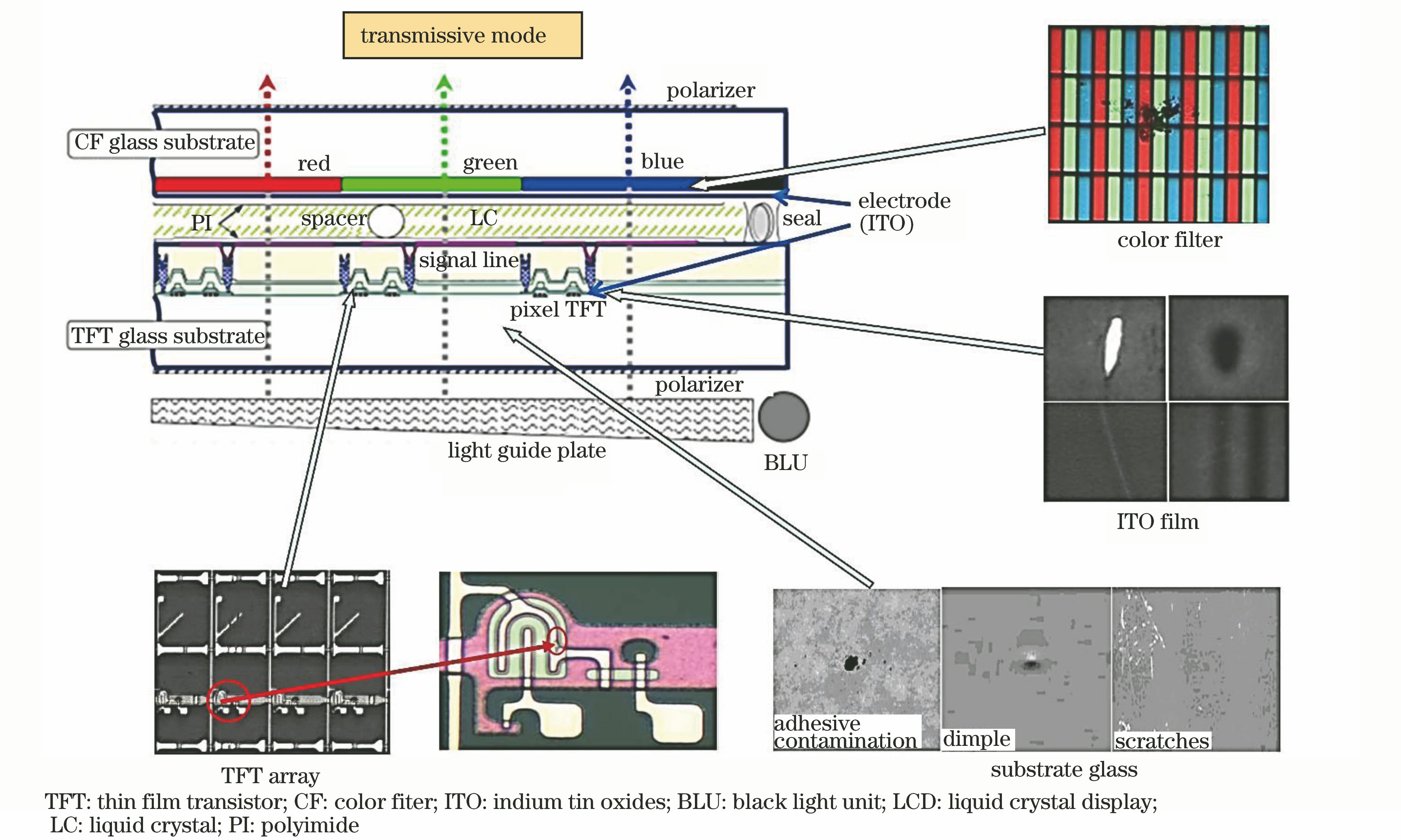
Fig. 1. Schematic diagram of the structure of TFT-LCD module and the defects on different layers
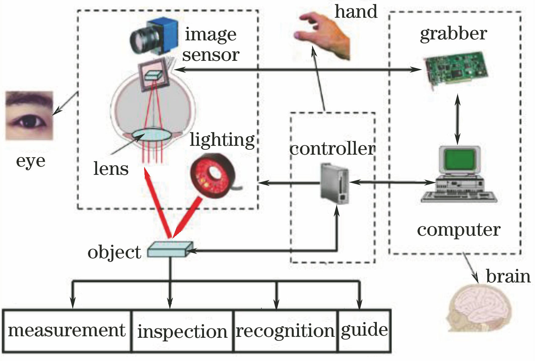
Fig. 2. AOI basic principle
Fig. 3. Schematic diagram of multi-sensor AOI system
Fig. 4. Schematic diagram of AOI system structure for inspecting TFT and filter array substrates
Fig. 5. Angle resolution inspection with the techniques of spot canning and multi-channel imaging.(a) Multi-channel scanning imaging principle; (b) image from a document scanner; (c) surface patterns obtained by point scanning with dark field imaging; (d) surface oil stain and fingerprint pattern obtained by point scanning with low angle imaging; (e) surface gradient map obtained by spot scanning with coaxial brightfield imaging
Fig. 6. Principle architecture of block parallel high-speed processing
Fig. 7. Schematic diagram of on-line AOI system mechanism for inspecting mobile backlight model
Fig. 8. Light scattering model on surface
Fig. 9. Typical lighting types. (a) Brightfield lighting; (b) axial brightfield lighting; (c)darkfield lighting; (d) low angle darkfield lighting; (e) diffuse lighting; (f) back lighting
Fig. 10. Comparison of different lighting effects. (a) Brightfield ring light illumination; (b) linear darkfield lighting with low angle; (c) brightfield ring lighting; (d) diffuse lighting
Fig. 11. Angle resolution relationship of surface defects of steel plate with camera and light source. (a) Angle relationship between camera and light; (b) angle resolution of defects
Fig. 12. Color disk showing warm and cool colors
Fig. 13. Lighting color, object feature color and imaging effects
Fig. 14. Imaging effect of red and blue illumination on aluminum alloy bottle cap. (a) Bottle cap to be inspected; (b) effect with red light illumination; (c) effect with blue light illumination
Fig. 15. Positions of ultraviolet, visible and infrared bands in electromagnetic spectrum
Fig. 16. Temperature and infrared radiation spectrum curve
Fig. 17. Comparison of visible and infrared spectra imaging
Fig. 18. Infrared imaging filtering effect. (a) Effect with white light; (b) effect with infrred light
Fig. 19. Infrared light penetration. (a) Effect using 660 nm red light; (b) effect using 880 nm infrared light
Fig. 20. Non thermal infrared vision and thermal infrared AOI technology
Fig. 21. Spectral distribution of UV-LED and mercury lamp
Fig. 22. Comparison of the ability of ultraviolet light to particle scattering. (a) 266 nm; (b) 470 nm; (c) 532 nm; (d) 633 nm
Fig. 23. Differential detection of spray paint on the car body with UV reflection method. (a) Same color presented under visible light; (b) color difference presented under ultraviolet light
Fig. 24. Principle of ultraviolet fluorescence detection
Fig. 25. Stokes shift
Fig. 26. Change of light vector on medium interface
Fig. 27. Reflection and transmission of light on metal surface
Fig. 28. Eliminating the influence of glare or bright spot on reflective surface by polarized imaging. (a) Image without polarizer; (b) image with polarizer
Fig. 29. Reflective polarized lighting and imaging
Fig. 30. Reflective images using ordinary lighting and polarized lighting, respectively. (a) Ordinary lighting; (b) polarized lighting
Fig. 31. Photoelastic effect. (a) Polarization image obtained by photoelastic method; (b) unfiltered image
Fig. 32. Stress and micro crack test with transmission polarization imaging
Fig. 33. Teledyne Dalsa 's four line CMOS polarization camera and imaging results. (a) Teledyne Dalsa's polarized camera; (b) stress measurement results
Fig. 34. Stokes parameter evaluation results
Fig. 35. Propagation characteristics of light in a vertical stratified fluid medium
Fig. 36. Schematic diagram of double field mirror schlieren measurement
Fig. 37. Practical two field mirrors schlieren measurement optical system
Fig. 38. Schematic diagram of direct shadow imaging
Fig. 39. Optical path of laser collimation lighting direct shadow imaging
Fig. 40. Optical path of focus shadow imaging
Fig. 41. Holographic interferometry in AOI. (a) Reference interferogram generation and recording; (b) speckle interference test process
Fig. 42. Five basic holographic interferograms of the surface defect. (a) Bull's eye; (b) groove; (c) bend; (d) displacement; (e) compression
Fig. 43. Digital holography scheme for large field of view
Fig. 44. Comparative digital holography. (a) Recording of a reference object hologram; (b) comparison of the measured object hologram with the reference object hologram
Fig. 45. Schematic diagram of ESPI digital speckle interferometry system
Fig. 46. Schematic diagram of shearing speckle interferometry system
Fig. 47. Shearing speckle interference system based on 4f optical system. (a)Principle of shearing speckle interference optical path based on 4f optical system; (b) traditional fringe pattern; (c) fringe pattern based on 4f optical system
Fig. 48. Defect inspection of aeronautical composite materials. (a) Defect specimen of multilayer composite honeycomb plate; (b) shearographic phase diagram of honeycomb plate defect
Fig. 49. Image processing of defect detection
Fig. 50. Schematic diagram of frequency domain filtering process
Fig. 51. Inspecting the fiber defects on a TFT array surface. (a) TFT array image with a fiber defect; (b) image removed periodic background; (c) pixel grey of the 92th row in time domain; (d) reconstruction results of the 92th row pixels
Fig. 52. TFT array singular value decomposition method. (a) TFT images with defects; (b) the first 10 singular values; (c) reconstructed image; (d) binary image
Fig. 53. Schematic diagram of CNN network architecture

Set citation alerts for the article
Please enter your email address
© Copyright 2018-2021 | Chinese Laser Press. All Rights Reserved 沪ICP备15018463号-20