
Ruijia Xu, Xiaocan Xu, Bo-Ru Yang, Xuchun Gui, Zong Qin, Yu-Sheng Lin, "Actively logical modulation of MEMS-based terahertz metamaterial," Photonics Res. 9, 1409 (2021)
- Photonics Research
- Vol. 9, Issue 7, 1409 (2021)
Abstract
1. INTRODUCTION
Metamaterials offer a strategy to artificially control electromagnetic waves on subwavelength scales and obtain unique optical response. Since the first experimental demonstration in 2000 [1], various metamaterial designs have attracted great interest due to their extraordinary properties, which cannot be found in traditional materials. Either the electric permittivity or magnetic permeability of metamaterials can be designed for desired application through the proper manipulation of the geometrical dimensions [2–6]. In general, they can be scaled to operate in the entire electromagnetic spectrum, including microwave [7], terahertz (THz) [8–12], infrared (IR) [13], and visible ranges [14]. With the rapid development of metamaterial, they have been reported in many fields, such as cloaking devices, thermophotovoltaics, microfluidic detection, and biomedical sensing [15–19].
Most current metamaterials can be passively controlled to perform a specific electromagnetic function. However, the active control for metamaterial designs has been desired to satisfy the requirements of real-world applications. As such, more and more researchers are paying attention to the active metamaterials via liquid crystal [20], laser pumping [21], phase transitions materials [22–24], and so on. However, many limitations exist among these tuning methods, owing to the nonlinear properties of natural materials. By artificially exploiting the electromagnetic force at the micro- and nanoscale, reconfigurable metamaterials are developed to achieve larger tuning range [25]. These reconfigurable metamaterials can be performed via the electromechanical method, i.e., micro-electro-mechanical systems (MEMS) technology [26–28]. MEMS-based metamaterials have been realized by using either an in-plane comb-drive actuator [29,30] or an out-of-plane bimorph actuator [31–33]. By using MEMS technology, the unit cell of metamaterial can be directly released and manipulated, which assists MEMS-based metamaterials to become candidates to help overcome the limitations of traditional tuning methods and provide an ideal platform for reconfigurable metamaterial.
For the reconfigurable capabilities of metamaterials, many researches have demonstrated the programmable metamaterial devices [34,35]. The optical programmable metamaterials are based on the electromagnetic switching response by using electromagnet [36], mechanical stretch [37], origami [38], and MEMS [39] methods, which have unlocked a new field for optical computing. However, most of these designs are only suitable for specific applications. To further increase the flexibility and applicability for the combo integration, the multifunctional characteristic is desired [40].
Sign up for Photonics Research TOC. Get the latest issue of Photonics Research delivered right to you!Sign up now
In this study, we numerically and experimentally demonstrate a design of reconfigurable metamaterial using a MEMS-based cantilever array to make the incident THz wave tunable. The proposed reconfigurable metamaterial is composed of a winding-shaped cantilever metamaterial (WCM) fabricated on silicon (Si) substrate. Herein, the multilayer cantilevers are used as an electrothermal actuator (ETA) as well as resonator. The composition of ETA is photoresist
2. DESIGN AND METHOD
Actuation of the proposed WCM devices is based on the thermal mismatch of different material components. Figure 1(a) shows schematic diagrams of a MEMS-based WCM device. The released ETA array is bent upward to realize the platform for various kinds of tunable 3D metamaterials. The geometrical denotations of the MEMS-based WCM device are indicated in Fig. 1(b). Herein, the corresponding parameters are
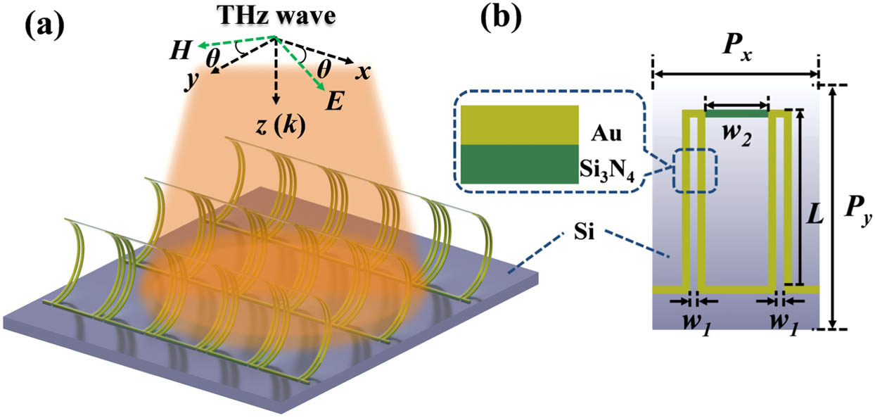
Figure 1.Schematic drawings of (a) MEMS-based winding-shaped cantilever metamaterial (WCM) and (b) the geometrical denotations of the WCM unit cell.
3. RESULTS AND DISCUSSIONS
To further study the electrical and mechanical properties of a MEMS-based WCM device, the relationship between cantilever height and applied DC bias voltage is investigated. By applying a DC bias voltage, the released ETA can be bent downward to the Si substrate. The relationship of cantilever heights and the applied DC bias voltages is summarized in Fig. 2(a). The inserted optical images illustrate the bending deformations of a MEMS-based WCM device under different DC bias voltages. The initial state of the WCM device is bent upward and keeps unchanged until the applied DC bias voltage of 10 V. It can be clearly observed that the ETA is bent downward gradually and the cantilever height decreases by increasing the driving voltage to 20 V. The radius of curvature of the cantilever becomes smaller simultaneously, along with the cantilever bending downward. In the driving DC bias voltage from 0 to 12 V, the applied voltages do not reach the actuation point of ETA, and the ETA height keeps stable without moving downward. There is minor change caused from the measurement deviation. When the driving voltage reaches the actuation voltage of the ETA, the ETA begins to bend downward, and then the ETA height decreases. According to Eq. (3), the cantilever height is proportional to the driving voltage. A linear relationship of cantilever height and applied DC bias voltage is in the voltage range of 13 to 21 V, which is defined as the work region of a MEMS-based WCM device. The cantilever height decreases from 273 to 86 μm. The vertical moving distance is 187 μm. The cantilever always suffers the snapping down on the substrate when the driving voltage reaches the pull-in voltage, which is a drawback for most MEMS devices. Figures 3(a) and 3(b) show the SEM images of a MEMS-based WCM array and unit cell, respectively. The exposed Si substrate surface was patterned by using inductively coupled plasma etching isotopically, which makes the Si substrate surface textured roughly, as observed in the SEM image of Fig. 3(b). Therefore, the reconfigurable characteristic of a MEMS-based WCM device is realized as the side view of the SEM image, as shown in Fig. 3(c). The composition of the WCM device is
![]()
Figure 2.Relationship of cantilever heights and the applied DC bias voltages. Inserted optical images illustrate the bending deformations of MEMS-based WCM device under different DC bias voltages.
![]()
Figure 3.SEM images of MEMS-based WCM device. Top views of MEMS-based WCM (a) array and (b) unit cell. (c) Side view of MEMS-based WCM device. (d) Composition of WCM single-cantilever.
The proposed tunable 3D metamaterial is formed through a MEMS process and can serve as a THz optical resonator. Such a design shows obvious asymmetric structure and exhibits polarization-dependent characteristics. Figures 4(a) and 4(b) show the simulated and measured transmission spectra of a MEMS-based WCM device without driving DC bias voltage, respectively. The polarization angle is defined as the intersection angle between the E-field and
![]()
Figure 4.(a) Simulated and (b) measured transmission spectra of MEMS-based WCM device without driving voltages at different incident polarization angles.
Since the optical properties of metamaterial are determined via manipulation of the geometrical dimensions, the transmission spectra of the proposed WCM devices can be tuned by exploiting the deformation of ETAs. The simulated and measured results for the influences of driving different DC bias voltages on the transmission spectra of MEMS-based WCM device are summarized in Fig. 5. At the condition of
![]()
Figure 5.(a)–(c) Simulated and (d)–(f) measured transmission spectra of MEMS-based WCM device at different driving voltages for polarization angles of (a), (d)
The optical switching performance is a key parameter for the THz switching function. To evaluate the optical switching performance of the MEMS-based WCM device, the switching ratio is defined as the resonant intensity at the condition of
![]()
Figure 6.Optical switching performances of MEMS-based WCM device operating at different driving voltages and monitoring at (a) 0.33 THz and (b) 0.88 THz.
The MEMS-based WCM device shows obvious dual-resonance and polarization-dependent characteristics. These characteristics can be expressed as optical signals for “on” and “off” states, which can be used in the opto-logic operation application. Such varied transmission signals need to be received by an integrated detector. To detect the modulated optical signals from a MEMS-based WCM device, a programmable device is proposed with an integration of the MEMS-based WCM device and metamaterial perfect absorber (MPA), as illustrated in Fig. 7(a). The MPA is fabricated by using a superposition of a split-ring resonator (SRR) and cross-shaped resonator (CR) on an Au mirror layer sandwiched by a dielectric spacer. For MPA, the absorption (
![]()
Figure 7.(a) Schematic drawings of MEMS-based WCM device integrated with MPA. Absorption spectra of (b) SRR, (c) CR, and (d) MPA. Insert images are drawings of unit cells. The geometrical dimensions are defined as
The optical detection performances of the programmable device integrated with the MEMS-based WCM device and MPA at 0.33 and 0.88 THz are further discussed. Figure 8(a) shows the absorption efficiency (AE) of the programmable device for the polarization angle
![]()
Figure 8.AE of programmable device for the polarization angle of (a)
By exploiting the optical performance of WCM devices at 0.33 and 0.88 THz, the logic operations of “OR” and “AND” gates can be simultaneously performed. Figure 9 summarizes the logic functions of the proposed programmable device integrated with a MEMS-based WCM device and MPA. The logical operation function of the “OR” gate is realized at 0.33 THz, as shown in Fig. 9(a). Two external input signals are the incident polarization angle and driving DC bias voltage. Herein, the input conditions of polarization angles for
![]()
Figure 9.Programmable device is functionalized as logic (a) OR and (b) AND gates. They are working at the frequency of 0.33 THz and 0.88 THz, respectively.
The large tuning range of resonance is a key factor for logical modulation of a THz device. The proposed MEMS-based WCM device provides an ideal platform to implant various kinds of metamaterial configurations on the central area of a WCM platform. Herein, a typical metamaterial configuration, i.e., electric spilt-ring resonator (eSRR) is chosen to be integrated into the MEMS-based WCM device as the SEM image shows in Fig. 10(a). The eSRR pattern is fabricated on the dielectric
![]()
Figure 10.SEM images of eSRR-WCM (a) unit cell and (b) array. (c) The measured transmission spectra of eSRR-WCM at (c)
4. CONCLUSION
In conclusion, a MEMS-based WCM device is demonstrated to realize a high-efficient optical switch, VOA, and programmable device. By driving an external voltage, the released cantilevers will be bent downward to the Si substrate surface. The resonant intensity at 0.33 THz decreases from 71% to 22% by changing the polarization angle from 0° to 90°. Moreover, the resonant intensity could be tuned by driving different bias voltage to perform the optical switch and VOA applications. The combination of changing polarization angle and driving bias voltage realizes the MEMS-based WCM device to exhibit the programmable characteristic. The MEMS-based WCM device shows better optical switching performance under the condition of polarization angle
Acknowledgment
Acknowledgment. The authors acknowledge the State Key Laboratory of Optoelectronic Materials and Technologies of Sun Yat-sen University for the use of experimental equipment.
References
[1] J. B. Pendry. Negative refraction makes a perfect lens. Phys. Rev. Lett., 85, 3966-3969(2000).
[2] D. R. Smith, J. B. Pendry, M. C. K. Wiltshire. Metamaterials and negative refractive index. Science, 305, 788-792(2004).
[3] C. M. Watts, X. L. Liu, W. J. Padilla. Metamaterial electromagnetic wave absorbers. Adv. Mater., 24, OP98-OP120(2012).
[4] Y. X. Cui, K. H. Fung, J. Xu, H. J. Ma, Y. Jin, S. L. He, N. X. Fang. Ultrabroadband light absorption by a sawtooth anisotropic metamaterial slab. Nano Lett., 12, 1443-1447(2012).
[5] M. M. Hossain, B. H. Jia, M. Gu. A metamaterial emitter for highly efficient radiative cooling. Adv. Opt. Mater., 3, 1047-1051(2015).
[6] W. Li, U. Guler, N. Kinsey, G. V. Naik, A. Boltasseva, J. G. Guan, V. M. Shalaev, A. V. Kildishev. Refractory plasmonics with titanium nitride: broadband metamaterial absorber. Adv. Mater., 26, 7959-7965(2014).
[7] D. Schurig, J. J. Mock, B. J. Justice, S. A. Cummer, J. B. Pendry, A. F. Starr, D. R. Smith. Metamaterial electromagnetic cloak at microwave frequencies. Science, 314, 977-980(2006).
[8] H. T. Chen, W. J. Padilla, J. M. O. Zide, A. C. Gossard, A. J. Taylor, R. D. Averitt. Active terahertz metamaterial devices. Nature, 444, 597-600(2006).
[9] X. Xu, R. Xu, Y.-S. Lin. Tunable terahertz double split-ring metamaterial with polarization-sensitive characteristic. Opt. Laser Technol., 141, 107103(2021).
[10] Y. Wen, K. Chen, Y.-S. Lin. Terahertz metamaterial resonator with tunable Fano-resonance characteristic. Results Phys., 23, 104049(2021).
[11] F. Lu, H. Ou, Y.-S. Lin. Reconfigurable terahertz switch using flexible L-shaped metamaterial. Opt. Lett., 45, 6482-6485(2020).
[12] W. Yang, Y.-S. Lin. Tunable metamaterial filter for optical communication in the terahertz frequency range. Opt. Express, 28, 17620-17629(2020).
[13] Y. Zhang, P. Lin, Y.-S. Lin. Tunable split-disk metamaterial absorber for sensing application. Nanomaterials, 11, 598(2021).
[14] Y.-S. Lin, J. Dai, Z. Zeng, B.-R. Yang. Metasurface color filters using aluminum and lithium niobate configurations. Nanoscale Res. Lett., 15, 77(2020).
[15] Y.-S. Lin, Z. Xu. Reconfigurable metamaterials for optoelectronic applications. Int. J. Optomechatron., 14, 78-93(2020).
[16] D. Zheng, Y.-S. Lin. Tunable dual-split-disk resonator with electromagnetically induced transparency characteristic. Adv. Mater. Technol., 5, 2000584(2020).
[17] X. J. Ni, Z. J. Wong, M. Mrejen, Y. Wang, X. Zhang. An ultrathin invisibility skin cloak for visible light. Science, 349, 1310-1314(2015).
[18] H. Ou, F. Lu, Z. Xu, Y.-S. Lin. Terahertz metamaterial with multiple resonances for biosensing application. Nanomaterials, 10, 1038(2020).
[19] R. Xu, Y.-S. Lin. Tunable infrared metamaterial emitter for gas sensing application. Nanomaterials, 10, 1442(2020).
[20] D. Shrekenhamer, W. C. Chen, W. J. Padilla. Liquid crystal tunable metamaterial absorber. Phys. Rev. Lett., 110, 177403(2013).
[21] M. Gupta, Y. K. Srivastava, R. Singh. A toroidal metamaterial switch. Adv. Mater., 30, 1704845(2018).
[22] R. N. Dao, X. R. Kong, H. F. Zhang, X. L. Tian. A tunable ultra-broadband metamaterial absorber with multilayered structure. Plasmonics, 15, 169-175(2020).
[23] K. Appavoo, R. F. Haglund. Detecting nanoscale size dependence in VO2 phase transition using a split-ring resonator metamaterial. Nano Lett., 11, 1025-1031(2011).
[24] H. Wang, Y. Yang, L. P. Wang. Switchable wavelength-selective and diffuse metamaterial absorber/emitter with a phase transition spacer layer. Appl. Phys. Lett., 105, 071907(2014).
[25] J. Y. Ou, E. Plum, J. F. Zhang, N. I. Zheludev. Giant nonlinearity of an optically reconfigurable plasmonic metamaterial. Adv. Mater., 28, 729-733(2016).
[26] X. Hu, Y.-S. Lin. Programmable terahertz metamaterial with multiple logic characteristics. Results Phys., 18, 103267(2020).
[27] Y. Han, J. Lin, Y.-S. Lin. Tunable metamaterial-based silicon waveguide. Opt. Lett., 45, 6619-6622(2020).
[28] Z. Xu, Y.-S. Lin. A stretchable terahertz parabolic-shaped metamaterial. Adv. Opt. Mater., 7, 1900379(2019).
[29] T. Xu, X. Xu, Y.-S. Lin. Tunable terahertz free spectra range using electric split-ring metamaterial. J. Microelectromech. Syst., 30, 309-314(2021).
[30] T. Xu, R. Xu, Y.-S. Lin. Tunable terahertz metamaterial using electrostatically electric split-ring resonator. Results Phys., 19, 103638(2020).
[31] R. Xu, Y.-S. Lin. Reconfigurable multiband terahertz metamaterial using triple-cantilevers resonator array. J. Microelectromech. Syst., 29, 1167-1172(2020).
[32] F. Zhan, Y.-S. Lin. Tunable multiresonance using complementary circular metamaterial. Opt. Lett., 45, 3633-3636(2020).
[33] R. Xu, Y.-S. Lin. Flexible and controllable metadevice using self-assembly MEMS actuator. Nano Lett., 21, 3205-3210(2021).
[34] Z. Xu, Z. Lin, S. Cheng, Y.-S. Lin. Reconfigurable and tunable terahertz wrench-shape metamaterial performing programmable characteristic. Opt. Lett., 44, 3944-3947(2019).
[35] Y. Liao, Y.-S. Lin. Reconfigurable terahertz metamaterial using split-ring meta-atoms with multifunctional electromagnetic characteristics. Appl. Sci., 10, 5267(2020).
[36] Z. W. Wang, Q. Zhang, K. Zhang, G. K. Hu. Tunable digital metamaterial for broadband vibration isolation at low frequency. Adv. Mater., 28, 9857-9861(2016).
[37] K. J. Fu, Z. H. Zhao, L. H. Jin. Programmable granular metamaterials for reusable energy absorption. Adv. Funct. Mater., 29, 1901258(2019).
[38] H. B. Fang, S. C. A. Chu, Y. T. Xia, K. W. Wang. Programmable self-locking origami mechanical metamaterials. Adv. Mater., 30, 1706311(2018).
[39] F. Zhu, Y.-S. Lin. Programmable multidigit metamaterial using terahertz electric spilt-ring resonator. Opt. Laser Technol., 134, 106635(2021).
[40] D. H. Le, S. Lim. Four-mode programmable metamaterial using ternary foldable origami. ACS Appl. Mater. Interfaces, 11, 28554-28561(2019).
[41] M. Shavezipur, W. J. Gou, C. Carraro, R. Maboudian. Characterization of adhesion force in MEMS at high temperature using thermally actuated microstructures. J. Microelectromech. Syst., 21, 541-548(2012).


Set citation alerts for the article
Please enter your email address

© Copyright 2018-2021 | Chinese Laser Press. All Rights Reserved 沪ICP备15018463号-20