
Zongyi Zhang, Yonggang Wu, Zihuan Xia, Jian Zhou, Xuefei Qin. Tunable reducibility of Brillouin zone and bandgap width in elliptical nanowire arrays[J]. Chinese Optics Letters, 2020, 18(6): 063601
- Chinese Optics Letters
- Vol. 18, Issue 6, 063601 (2020)
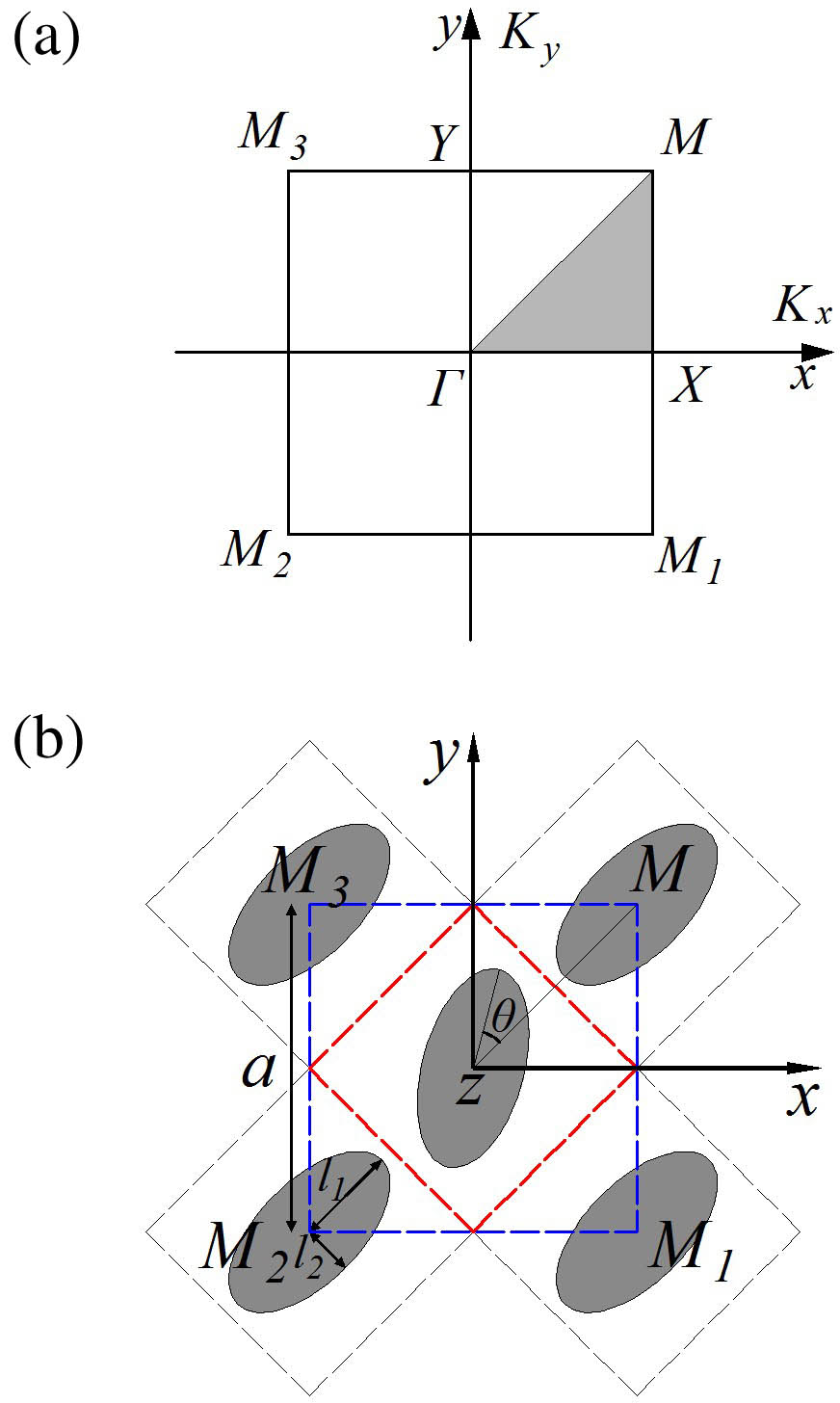
Fig. 1. (a) 1BZ diagram of the tetragonal lattice; (b) the section of the elliptical nanowire array primitive cell model.
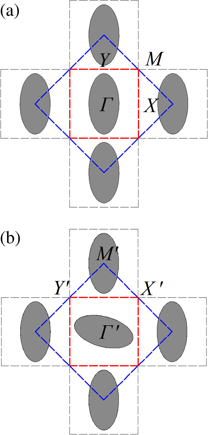
Fig. 2. Comparison of the central elliptical nanowires (a) before and (b) after rotation.
Fig. 3. TE and TM modes band structure calculated along the high symmetry lines (a) for
Fig. 4. Stereograms of (a) band 1, (b) band 2, (c) band 3, and (d) band 4 that are calculated in the whole first BZ for the parallel elliptical nanowires array. The band values are projected to the plane of
Fig. 5. Contour map of the four lowest TE mode energy bands of the PC when
Fig. 6. Contour map of the four lowest TM mode energy bands of the PC when
Fig. 7. First TE mode bandgap width of the arrays with the central element under different rotation angles.
Fig. 8. (a) Contour map of the four lowest TE mode energy bands of the perpendicular elliptical nanowires arrays at different rotations. The first, second, and third rows are array diagrams and energy bands rotated with respect to the 5 by 15°, 30°, and 45°. (b) The first TE mode bandgap width of the perpendicular arrays under different rotation angles.

Set citation alerts for the article
Please enter your email address
© Copyright 2018-2021 | Chinese Laser Press. All Rights Reserved 沪ICP备15018463号-20