Rotating elliptical nanowire arrays as two-dimensional photonic crystals has been proposed and studied in this Letter. The analysis of the four lowest energy bands and the first bandgap width of some examples illustrates that the rotation and configuration of the primitive cell can have effects on the reducibility of the Brillouin zone. As the central element’s orientation changes, the irreducible Brillouin zone could be expanded to the whole first Brillouin zone. Special attention has been paid to the nanowire arrays with adjacent elements perpendicular to each other, and the irreducible Brillouin zone unexpectedly retracted back to the 1/8 of the first Brillouin zone though the symmetry of elements is lower than that of the square lattice. Meanwhile, the first bandgap width of the perpendicular array can be adjusted by the rotation of each primitive element.
The physical concept of photonic crystals (PCs) was first proposed independently by Yablonovitch[1] and John[2] in 1987. Many concepts used in solid-state physics for semiconductors are also applicable to photonic crystals, such as Brillouin zone (BZ), irreducible Brillouin zone (IBZ), Bloch wave[3], and dispersion relation[4]. The application of photonic crystals is mainly based on the existence of the photonic bandgap, such as controlling light flow with a line-defect PC[5–7] and photon bunching[8]. One of the bottlenecks to generate a photonic bandgap is the degeneracy of highly symmetric points in the Brillouin zone of photonic crystals. It is a consensus to change the symmetry of photonic crystals to separate the degenerate states. Thus, various photonic crystal structures are designed to optimize the bandgap[9–18]. However, the properties of the orientation of PC scatterers have barely been reported. For a long time, the discussions were restricted to the dielectric scatterers of a perfect rotational symmetry ( circular symmetry). Representative examples include dielectric rods in a square or triangular lattice in a two-dimensional (2D) photonic crystal system. For such scenarios, the dielectric scatterers have a higher-order symmetry than the overall lattice (i.e., circular symmetry four-fold rotational symmetry in a square lattice or six-fold symmetry in a triangular lattice). It is well known that the first Brillouin zone (1BZ) can be reduced to only its fundamental constituent fraction driven by intrinsic geometrical symmetry. It is yet to be investigated that, when the scatterer symmetry is inferior to that of the overall lattice, whether the reducibility of the 1BZ still remains the same. To this end, we computationally studied 2D PCs with elliptical nanowires as the internal scatterers.
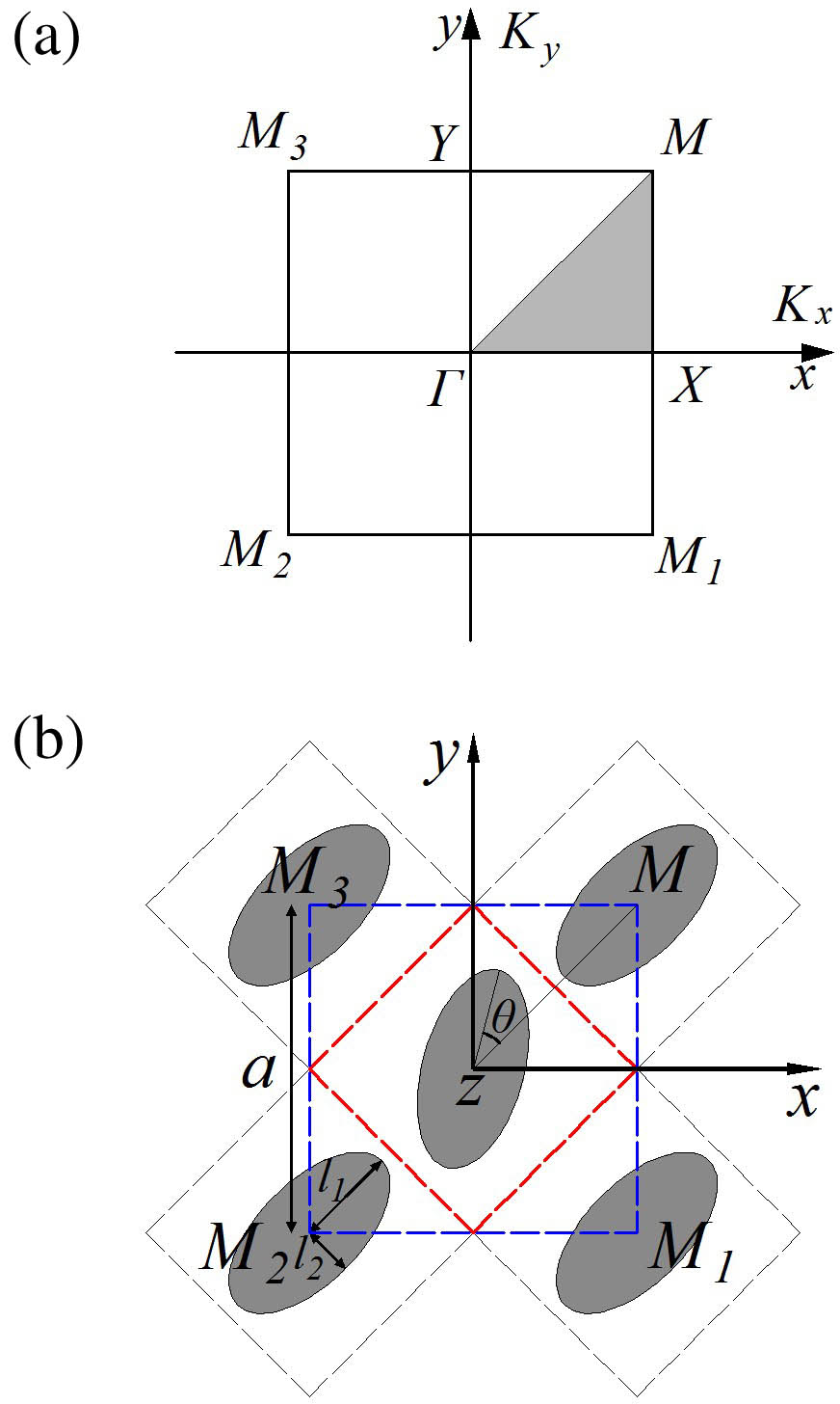
Figure 1(a) is a schematic diagram of the 1BZ (reduced Brillouin zone) of the tetragonal lattice[19]. Here , , , , , , and represent the symmetry points. , , etc. are the symmetry axis. The 1BZ can be divided into 8 equivalent zones according to the symmetry of the point group of the crystal. Under normal conditions, only one of the eight equivalent zones has to be calculated, the triangular shaded zone in Fig. 1(a), and then the full band information can be gotten. It must be made clear that this is only true under certain conditions where the symmetry of the primitive cell[20] element is higher than that of the lattice, and thus the primitive element can be abstracted into a point. In fact, the symmetry of the primitive cell elements as the photonic crystal scatterers can be designed to be lower than the symmetry of the lattice, and the orientation and configuration of the elements can be changed at will[21]. It makes the symmetry of the crystal different from the crystal lattice and the IBZ may change.
Figure 1.(a) 1BZ diagram of the tetragonal lattice; (b) the section of the elliptical nanowire array primitive cell model.
In this Letter, we choose low symmetry elliptical nanowires as the element, as shown in Fig. 1(b). In order to study the effects of the orientation change of the elliptical nanowire arrays on reducibility, the nanowire at the center of the primitive cell is rotated. Figure 1(b) is the section of the elliptical nanowire array primitive cell model. The crystalline silicon elliptical nanowires (with a relative permittivity of 11.9) are infinitely long in the -axis direction and are arranged in the air (with a relative permittivity of 1) with a square lattice. Relevant experimental silicon elliptical nanowire array fabrication methods can be referenced in the literature[22]. The ratio of the length of the major and minor axes of the ellipse , and the fill ratio . The elliptical nanowires located in the center of the primitive cell rotate an angle counterclockwise with respect to the parallel-oriented elliptical nanowires array, where is the lattice constant.
Sign up for Chinese Optics Letters TOC. Get the latest issue of Chinese Optics Letters delivered right to you!Sign up now
It is noteworthy that when the elliptical nanowires are arranged in a parallel orientation array, as shown in Fig. 2(a), the primitive cell region is in the red dashed box. While rotating the major axis (or minor axis) orientation of the central elliptical nanowires, as shown in Fig. 2(b), the primitive cell region of the new array expands into the blue dashed box.
Figure 2.Comparison of the central elliptical nanowires (a) before and (b) after rotation.
We set the lattice positions , , , and in the red box and , , , and in the blue box with the methods of solid-state physics. As we can see in Fig. 2(a), for the parallel orientation ellipse nanowire array, the selected wave vector paths along the , , , , and directions are not the same. This means that the complete bandgap can be described only by calculating the zone for the parallel orientation ellipse nanowire array. However, when it comes to the rotated elliptical nanowire arrays, as shown in Fig. 2(a), the original zone no longer applies since the wave vector paths along the , , , , and directions are also not all the same. A larger zone may help us get a completely new bandgap structure diagram. That is to say, the IBZ changes when the orientation of the elliptical nanowire arrays changes.
In order to verify the above inference, the plane wave expansion (PWE) method[3,23] is used to calculate the whole 1BZ. Only the central nanowire in each primitive cell rotates counterclockwise while the four nanowires at the four corners do not rotate. Considering rotation symmetry and structural similarity in geometry, the bandgap structures can only be calculated when the central nanowire’s rotation angle , which is 0°, 15°, 30°, 45°, 60°, 75°, and 90°, respectively. For 2D PCs, when the electromagnetic wave propagates along the direction perpendicular to the axial direction of the elements ( plane in this Letter), the electromagnetic field is the linear superposition of two decomposed polarization modes, and (TE mode and TM mode), and their field vectors are parallel and perpendicular to the axial direction of the elements, respectively. Because these two modes are independent of each other, they can be discussed separately. In this study, the results of both two modes are given.
The eigenfrequency values of the TE or TM mode are also calculated by PWE. The polarization mode of [or ] can be Fourier expanded according to Bloch theory and the Maxwell equation of [or ] can be reduced to the solution of the eigenvalue for [or ]: where is the Bloch wave vector, is the 2D reciprocal lattice, and is the reciprocal lattice expansion of the dielectric function . wave vectors are used to calculate the eigenfrequency distribution in the first BZ.
Figure 3 is the calculated TE and TM mode band structure of nanowire arrays along high symmetry lines in Fig. 2, where Fig. 3(a) is for and Fig. 3(b) is for . The lowest four bands[24] are indicated in black solid lines and red dashed lines for the TE mode and TM mode, respectively. The horizontal coordinate is the path of . Because the first BZs of the two structures are different, the symmetry points are marked with different characters. The vertical coordinate is the scaling frequency . Note that the bandgap can be only found in the TE mode. It suggests that these PCs can be used to form the single-polarization photonic waveguide, which may tremendously enable the study of the few-photon scattering process, including single-photon super-radiance excitation[25], order-of-magnitude enhancement of the two-photon[26], and the few-photon scattering loss mechanism[27]. By comparing the maximum and minimum values of each band in the TE mode, it can be found that the first bandgap appears between the first band and the second band (shown in the shaded part of the figure) for the parallel elliptical nanowires array, while the first bandgap appears between the second band and the third band for the perpendicular elliptical nanowires array. Obviously, the bandgap value of the perpendicular elliptical nanowires array () is much more than that of the parallel ones (), almost 3 times. It seems that the rotation causes the second band to separate from the third band, the first band and the second band to partially merge, and the third band and the fourth band to partially merge. Such merge should be the degeneracy of the transmission bands along and caused by orientation. It should be noted that when , the paths along and are the same, as well as the and paths. However, there is no degeneracy for the transmission bands along and . According to Fig. 2(a), the zone can sufficiently describe the first BZ of the parallel elliptical nanowires array. However, for the perpendicular elliptical nanowires array, the zone could be redundant since a high symmetry can be found in Fig. 3(b). and are symmetrical, and and are symmetrical, respectively. In other words, the (or ) zone could be the IBZ when . The above phenomenon can also be observed in the TM mode. In addition, the bands’ positions in the TM mode are generally higher than that in the TE mode, although there is no bandgap in the TM mode. We believe that the central element orientation has an important effect on the reducibility of BZ.
Figure 3.TE and TM modes band structure calculated along the high symmetry lines (a) for and (b) for .
Figure 4 shows the complete stereogram of the TE band structure calculated in the first BZ for the parallel elliptical nanowires array. Figures 3(a)–3(d) are stereograms of bands 1–4, respectively, and correspond to the band in Fig. 3(a) (black solid lines). The bottom surface of each figure in Fig. 4 is the wave vector plane. In this Letter, is only evaluated in the first BZ .
Figure 4.Stereograms of (a) band 1, (b) band 2, (c) band 3, and (d) band 4 that are calculated in the whole first BZ for the parallel elliptical nanowires array. The band values are projected to the plane of to form a contour map at the bottom.
To confirm the hypothesis, the bandgap structures in the whole first BZ for different oriented arrays are calculated, and the band values are projected to the plane of to form a contour map. The band value increases as the color changes from blue to red. Each band’s maximum and minimum in the whole first BZ are marked with a black point and a white point, respectively. When the orientation of the elliptical nanowires array is parallel, the energy bands at all levels maintain a double axisymmetric ( axis and axis) or a distribution, as shown in Figs. 5(a1)–5(a4). So, calculation of the zone’s bandgap, which is a quarter of , can be the complete first BZ. But for arrays with a central element rotation orientation, the zone’s bandgap characteristics cannot fully represent the first BZ’s bandgap structure.
Figure 5.Contour map of the four lowest TE mode energy bands of the PC when is 0°, 15°, 30°, 45°, 60°, 75°, and 90°. (a1)–(g1) band 1, (a2)–(g2) band 2, (a3)–(g3) band 3, (a4)–(g4) band 4.
When rotates from 0° to 75°, the distribution of band 1 in the first BZ is almost unchanged, as shown in Figs. 5(b1)–5(f1). It can be explained that, in most cases, the wavelength is longer than the size of the scatterers, so the symmetry of the scatterer has no strong influence on the first band. The positions of the extreme values of band 2 remain unchanged, but the distribution over the first BZ has been slightly distorted, as shown in Figs. 5(b2)–5(f2). This distribution shift could be described as a rhombus shifting into a square. The extreme values of band 3 are shifted and the maximum value point moves out of the high symmetry lines and changes counterclockwise, as shown in Figs. 5(b3)–5(f3). The morphology of band 3 gradually changes from two approximately parallel linear shapes (red zones) into a cross shape at the center of the zone. The case of band 4 is similar to band 3 but its minimums tend to go clockwise and the maximums remain at the same positions. The distribution of band 4 tends to split from a rectangle into a larger square. For from 15° to 75°, most of the bands’ distribution shows a characteristic. The shift of extreme values in contour maps indicates that the original zone no longer applies and the IBZ develops into a larger zone, which is half of .
The perpendicular elliptical nanowires array’s bands, which are shown in Figs. 5(g1)–5(g4), are then added for comparison. The perpendicular elliptical nanowires array’s bands show a feature. That is to say, the IBZ can be reduced to the (or ) zone on this occasion, which strongly confirms our hypothesis. Figure 5 shows that with the increase of from 0° to 90°, the distribution of the energy band contour map at the four levels is a process of shifting of symmetry-asymmetry-symmetry and a transformation from to , then to . The IBZ develops into the whole first BZ during rotation but it narrows into 1/8 of the whole first BZ at the end. It conflicts with our traditional knowledge of solid-state physics, as the element has a lower symmetry compared to the lattice.
In addition, the contour maps of the TM mode are given in Fig. 6. A qualitative conclusion for the TM mode can be made that there is a similar result regarding the reducibility of the first BZ as the TE mode holds. Slightly different from the TE mode, the distribution of band 1 in the first BZ shows an obvious change in the process. This difference can be attributed to the fact that the polarization is much weaker than the polarization, so the symmetry of the scatterer has a strong influence on the first band of the TM mode. Still, with the increase of from 0° to 90°, the distribution of the energy-band contour map at the four levels transforms in a process as . The IBZ develops into the whole first BZ during rotation and narrows into 1/8 of as well. It can be concluded that this tunable reducibility of BZ is universal for both the TE and TM modes.
Figure 6.Contour map of the four lowest TM mode energy bands of the PC when is 0°, 15°, 30°, 45°, 60°, 75°, and 90°.
It is an extremely interesting and remarkable conclusion that the perpendicular elliptical nanowire array has the simplest IBZ, while its unit cell symmetry is lower than that of the parallel elliptical nanowires array. Geometrically speaking, the unit cell of the perpendicular elliptical nanowire array has no mirror symmetry, but the unit cell of the parallel elliptical nanowires array has two mirror symmetries. However, in terms of rotation operations, the former has a rotation axis while the latter only has a rotation axis. This indicates that the properties of the scatterer’s orientation have a more profound effect on the reducibility of the IBZ than the symmetry of the scatterer itself. It seems that a higher rotation maneuverability can lead to a more reduced BZ. This discovery could expand the understanding of IBZ in traditional solid-state physics. The orientation of scatterers provides a new idea for the design of PCs with specific functions.
The first bandgap width of these arrays with different values is shown in Fig. 7. As increases, the width increases significantly. This character can be used in an optical modulator[28–31] for a specific wavelength of light. The width broadening trend suggests that the perpendicular elliptical nanowires array has a unique character in the reducibility of BZ.
Figure 7.First TE mode bandgap width of the arrays with the central element under different rotation angles.
Furthermore, we simultaneously rotate every element in the primitive cell (with the center of each element as the rotation point), so that all adjacent primitive elements maintain orthogonal pointing relations with each other no matter how much rotation occurs. Given the rotational symmetry in orthogonal elliptical nanowire arrays, just three more arrays are picked that rotate 15°, 30°, and 45° relative to the perpendicular array in Fig. 5, respectively.
In Fig. 8(a), all the rotated orthogonal arrays show a highly symmetric band in the first BZ, which is similar to the array. That is to say that the rotation angle of the elements does not break the symmetry. For all the perpendicular elliptical nanowire arrays, there should be a stable and extremely high symmetry in the energy band. The IBZ can be reduced to 1/8 of the first BZ in these structures, though the symmetry of the elements is lower than that of the lattice, which breaks the traditional cognition in solid-state physics.
Figure 8.(a) Contour map of the four lowest TE mode energy bands of the perpendicular elliptical nanowires arrays at different rotations. The first, second, and third rows are array diagrams and energy bands rotated with respect to the array in Fig. 5 by 15°, 30°, and 45°. (b) The first TE mode bandgap width of the perpendicular arrays under different rotation angles.
Last, the first bandgap widths of the perpendicular elliptical nanowire arrays under different rotation angles are given in Fig. 8(b) as well. As the arrays’ primitive cell is more like a cross, the first bandgap width reduces. It proves that the perpendicular elliptical arrays can not only affect the reducibility of BZ, but also affect the regulation of the bandgap width. Our proposed orthogonal elliptic nanowire array structures has a greater prospect in PC applications than the highly ordered structures.
To sum up, energy band structures of 2D PCs with elliptical nanowires arranged in squares surrounded by air are studied in the whole first BZ. The rotation of the central elliptic nanowire element in each primitive cell has a remarkable effect on the reducibility of BZ and the first bandgap width of the structure. On the one hand, with a low symmetry scatterer as the primitive element, the IBZ can be expanded to the whole first BZ as the rotation changes. But to some angle, such as 90°, which makes the PC a perpendicular elliptical nanowires array, the IBZ shrinks back to the simplest form, 1/8 of the first BZ, as if the elliptical nanowires are reduced to points. The perpendicular elliptical nanowire arrays have a smallest IBZ, while the symmetry of the element is lower than that of the lattice. IBZ as defined in solid-state physics is not appropriate for the symmetry of the elements and for crystals whose orientation and configuration are variable. On the other hand, the orientation of the scatterers can affect the first bandgap width of the structure as well. PCs with a higher arrangement disorder have a larger gap width. When the parallel array rotates into an orthogonal array, the first bandgap width increases. When the perpendicular elliptical nanowire arrays rotate into a cross array, the first bandgap width decreases. It provides us with different rotation angles to adjust photons of different wavelengths to pass through the PCs. This special property makes the rotated elliptical nanowire arrays’ application more flexible[32–34].