• Infrared and Laser Engineering
  • Vol. 51, Issue 4, 20210399 (2022)
Junbin Li1, Aimin Liu2, Zhi Jiang1, Jin Yang1, Wen Yang1, Jincheng Kong1, Dongsheng Li1, Yanhui Li1, and Xuchang Zhou1
Author Affiliations
  • 1Kunming Institute of Physics, Kunming 650223, China
  • 2School of Physics, Dalian University of Technology, Dalian 116024, China
  • show less
    DOI: 10.3788/IRLA20210399 Cite this Article
    Junbin Li, Aimin Liu, Zhi Jiang, Jin Yang, Wen Yang, Jincheng Kong, Dongsheng Li, Yanhui Li, Xuchang Zhou. Analysis of dark current characteristic of InAs/GaSb superlattice longwave infrared detectors[J]. Infrared and Laser Engineering, 2022, 51(4): 20210399 Copy Citation Text show less
    Energy band alignment of pN hetero-junciton. (a) Without contact; (b) With contact
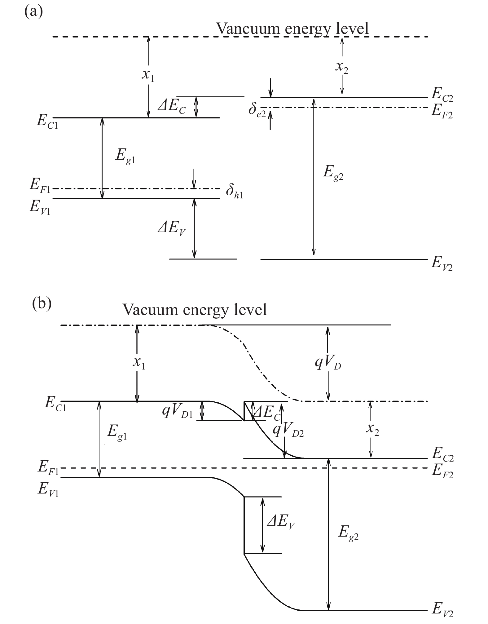
    Fig. 1. Energy band alignment of pN hetero-junciton. (a) Without contact; (b) With contact
    Schematic diagram of superlattice IR detector structure and its energy band alignment
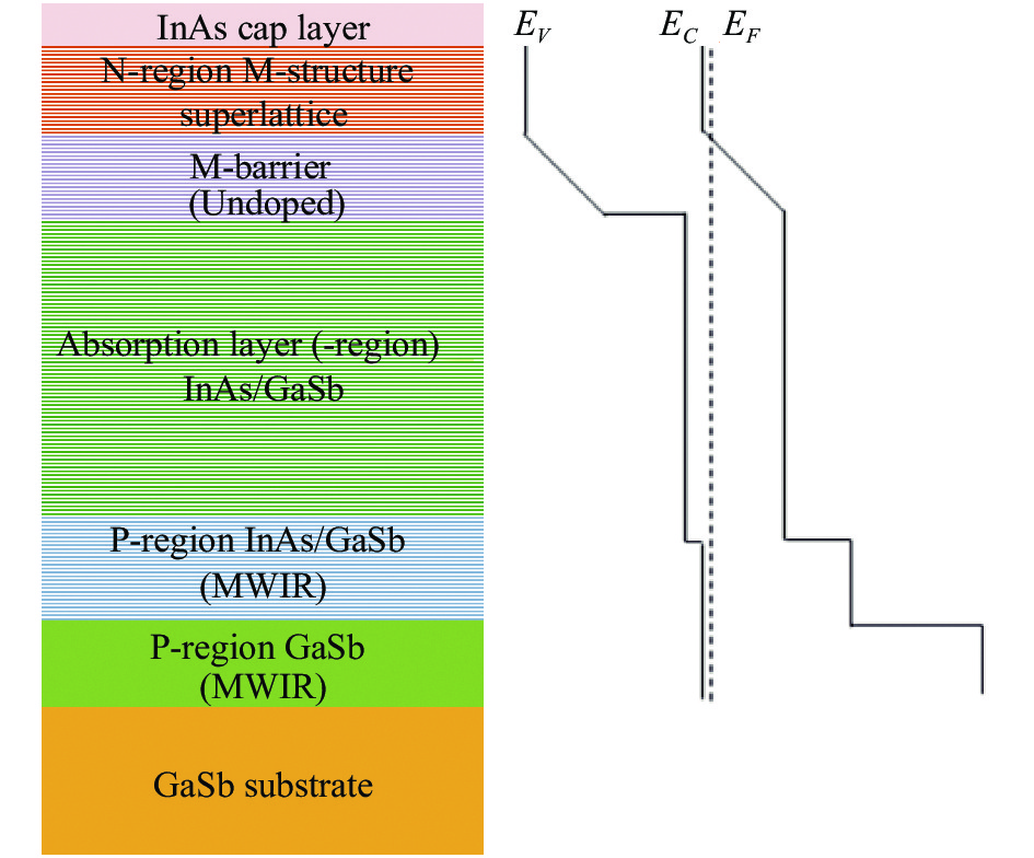
    Fig. 2. Schematic diagram of superlattice IR detector structure and its energy band alignment
    Dark currents of photodetector with different mesa sizes
    Fig. 3. Dark currents of photodetector with different mesa sizes
    The relationship between the inverse product of resistances with area at zero bias with perimeter/area of detectors
    Fig. 4. The relationship between the inverse product of resistances with area at zero bias with perimeter/area of detectors
    Measurement and fitting results of dark current of photodetector with 60 μm mesa size
    Fig. 5. Measurement and fitting results of dark current of photodetector with 60 μm mesa size
    G-R current and trap assisted tunnel current of photodetector with different doping density of absorption layer
    Fig. 6. G-R current and trap assisted tunnel current of photodetector with different doping density of absorption layer
    RegionSuperlattice periodThickness/nmDoping concentration/cm−3
    n-InAs cap layer--201×1018
    N-region18 mLs InAs/ 3 mLs GaSb/ 5 mLs AlSb/ 3 mLs5061×1018
    M-barrier18 mLs InAs/ 3 mLs GaSb/ 5 mLs AlSb/ 3 mLs506Unintentional doped (~2×10¹⁵)
    π-region 14 mLs InAs/ 7 mLs GaSb21822×1016
    P-region8 mLs InAs/ 8 mLs GaSb5861×1018
    P-GaSb--5001×1018
    Table 1. Key parameter of IR detector structure
    ParametersValue
    Hole effective mass (mh) 0.4 m0
    Electron effective mass (me) 0.04 m0
    Electron tunneling effective mass (mT) 0.04 m0
    Electron mobility2 000 cm2Vs−1
    Hole mobility200 cm2Vs−1
    Electron lifetime (τe) 30 ns
    GR lifetime (τGR) 30 ns
    Bandgap of absorption layer (Eg) 0.12 eV
    Trap energy level (Et) 3/4 Eg
    Dielectric constant (εs) 15.34 ε0
    Trap density (Nt) 2.1×1013 cm−3
    Doping density of absorption layer (NA) 2×1016 cm−3
    Doping density of barrier layer (ND) 2×1015 cm−3
    Table 2. Fitting parameters of model of dark current
    Junbin Li, Aimin Liu, Zhi Jiang, Jin Yang, Wen Yang, Jincheng Kong, Dongsheng Li, Yanhui Li, Xuchang Zhou. Analysis of dark current characteristic of InAs/GaSb superlattice longwave infrared detectors[J]. Infrared and Laser Engineering, 2022, 51(4): 20210399
    Download Citation