
Zhibo Xing, Wei Fan, Dajie Huang, He Cheng, Tongyao Du. High laser damage threshold reflective optically addressed liquid crystal light valve based on gallium nitride conductive electrodes[J]. High Power Laser Science and Engineering, 2022, 10(6): 06000e35
- High Power Laser Science and Engineering
- Vol. 10, Issue 6, 06000e35 (2022)
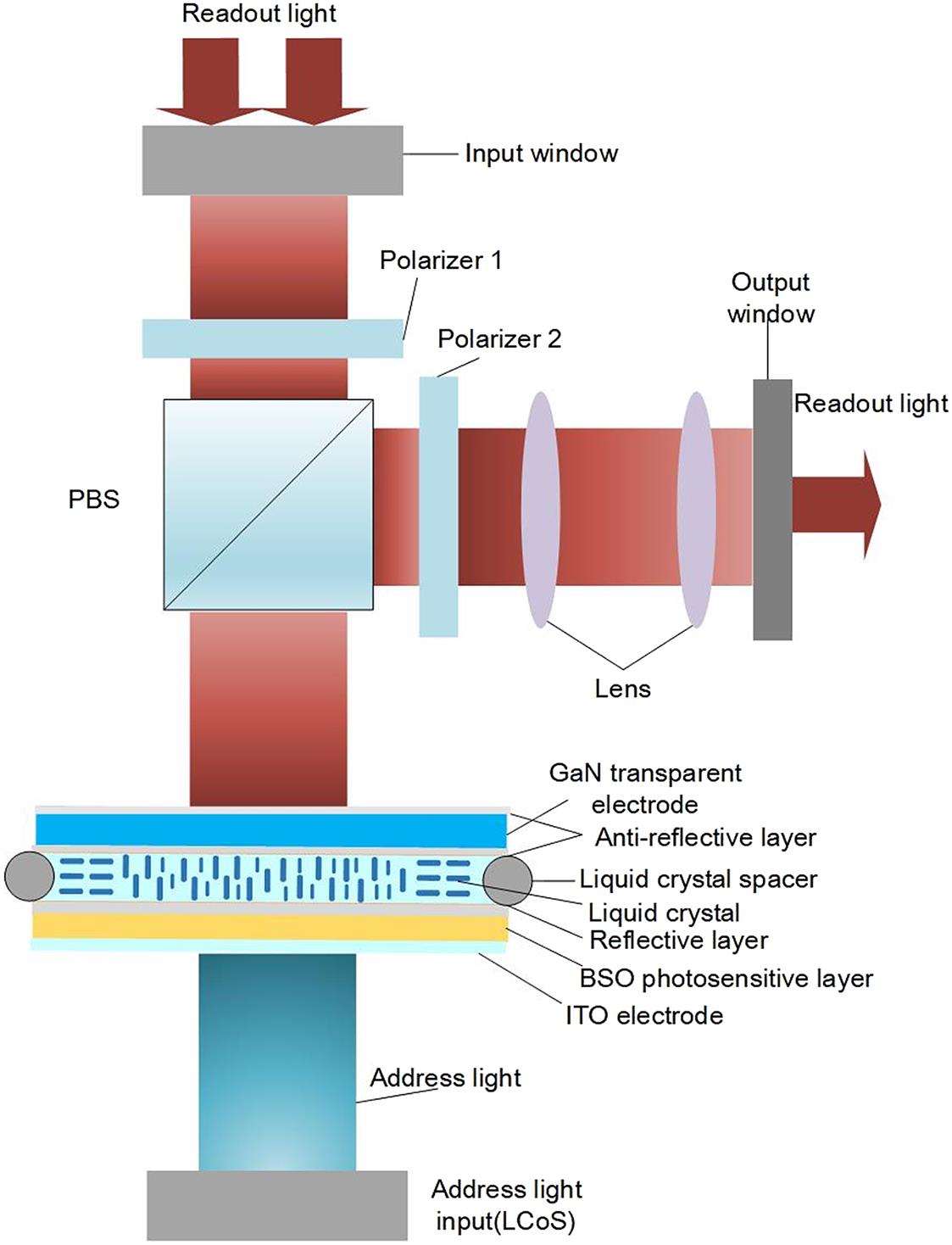
Fig. 1. The basic structure of the reflective OALCLV.
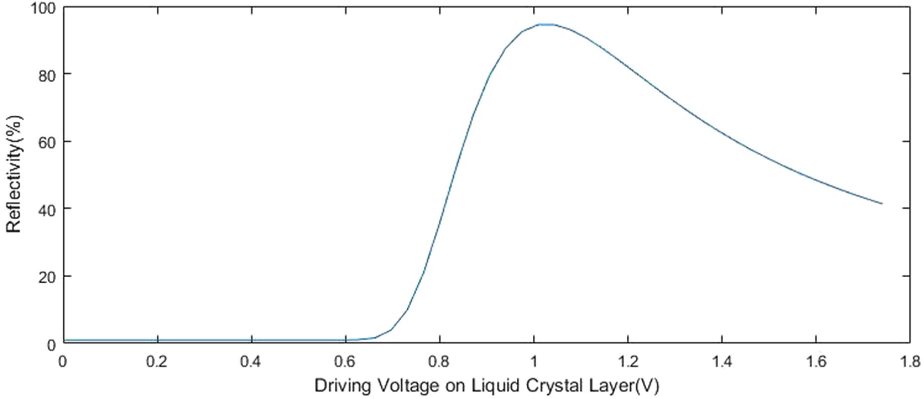
Fig. 2. The relationship between the driving voltage on the liquid crystal cell and the reflectivity of the OALCLV. Only the loss of the liquid crystal layer is considered; the other layers are considered as ideal materials.
Fig. 3. The relationship between the ratio of the voltage of the liquid crystal layer and the total voltage and the driving frequency in the (a) off-state and (b) the on-state.
Fig. 4. Schematic of the experimental facility used for the GaN damage resistance test.
Fig. 5. The laser damage data of the GaN single crystal. The experimental data of the damage probability are represented by discrete points, while the fitting data are represented by the linear fitting line.
Fig. 6. The damage spot micrograph of the GaN single crystal specimen (the measuring scale is shown in the figure).
Fig. 7. The image response of full black input (a) and full white input (b) of the OALCLV.
Fig. 8. The test result (rising curve (a) and declining curve (b)) of the response speed of the OALCLV.
Fig. 9. The image response test result of the reflective OALCLV: input ((a), (c)) and output ((b), (d)).
|
Table 1. The parameters in the simulation of the HFE mode reflective liquid crystal cell.
|
Table 2. The parameters of the liquid crystal cell in Equation (1) .
|
Table 3. The parameters in the damage resistance test of the GaN single crystal.
|
Table 4. The experimental setup and result of the reflective OALCLV.

Set citation alerts for the article
Please enter your email address
© Copyright 2018-2021 | Chinese Laser Press. All Rights Reserved 沪ICP备15018463号-20