• Chinese Journal of Lasers
  • Vol. 46, Issue 10, 1000001 (2019)
Yang Shi1, Bing Xu1、*, Dong Wu1, Yi Xiao3、**, Yanlei Hu1, and Chengli Yao2
Author Affiliations
  • 1School of Engineering Science, University of Science and Technology of China, Hefei, Anhui 230026, China
  • 2School of Chemistry and Chemical Engineering, Hefei Normal University, Hefei, Anhui 230601, China
  • 3School of Mechanical Engineering, Nantong Vocational University, Nantong, Jiangsu 226007, China
  • show less
    DOI: 10.3788/CJL201946.1000001 Cite this Article Set citation alerts
    Yang Shi, Bing Xu, Dong Wu, Yi Xiao, Yanlei Hu, Chengli Yao. Research Progress on Fabrication of Functional Microfluidic Chips Using Femtosecond Laser Direct Writing Technology[J]. Chinese Journal of Lasers, 2019, 46(10): 1000001 Copy Citation Text show less
    Schematicsof TPP processing. (a) TPA processing; (b) scheme of TPP fabrication; (c) illustration of achievement of sub-diffraction-limit (SDL) fabrication accuracy, in which absorption probabilities for single photon absorption (SPA) and TPA are denoted by dashed and solid lines, respectively, and inset is diffraction pattern
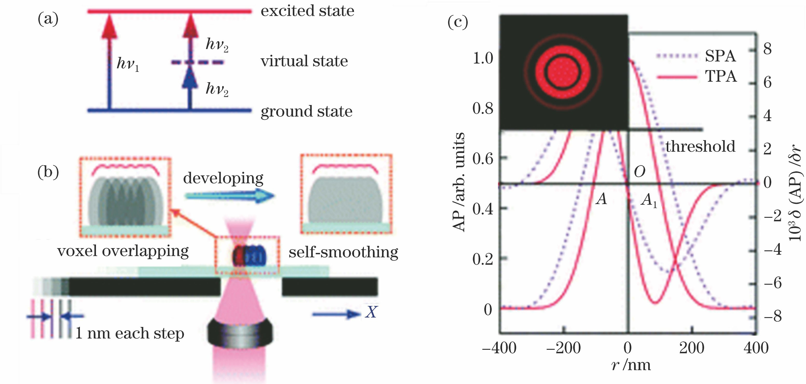
    Fig. 1. Schematicsof TPP processing. (a) TPA processing; (b) scheme of TPP fabrication; (c) illustration of achievement of sub-diffraction-limit (SDL) fabrication accuracy, in which absorption probabilities for single photon absorption (SPA) and TPA are denoted by dashed and solid lines, respectively, and inset is diffraction pattern
    TPP processing system
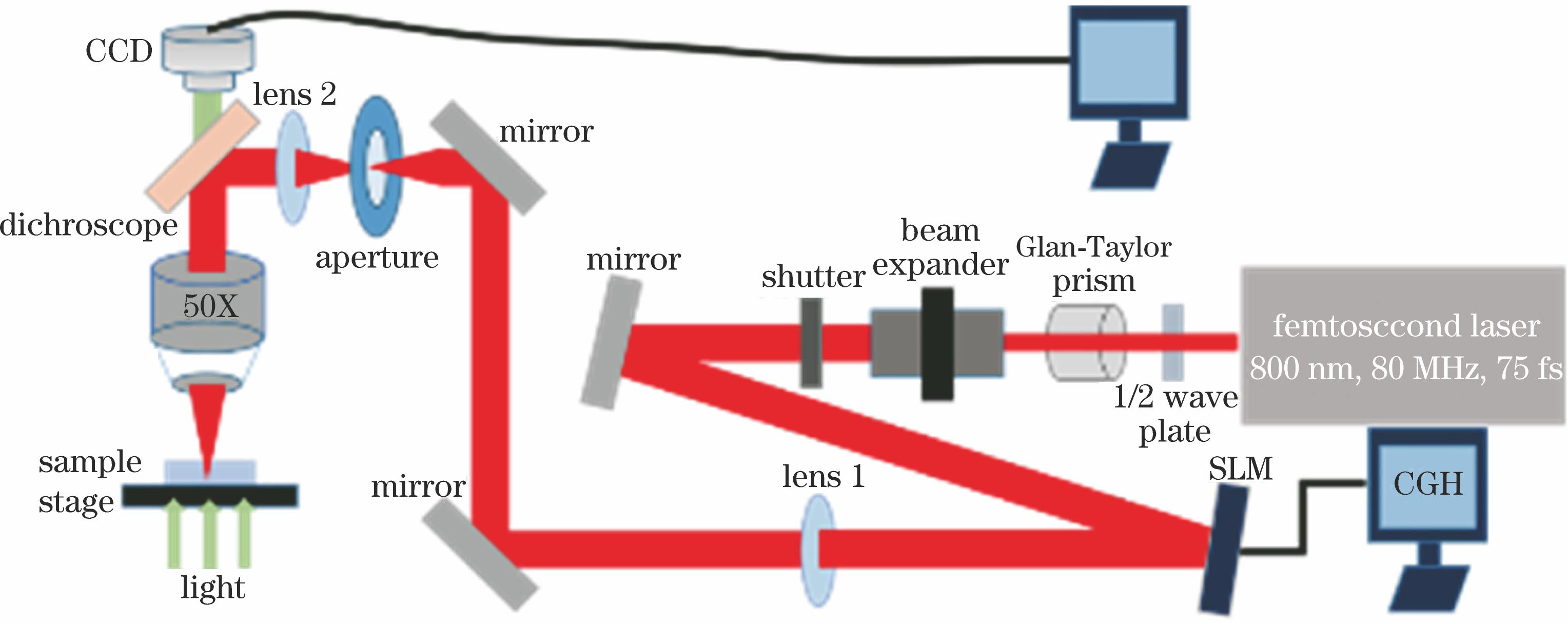
    Fig. 2. TPP processing system
    Different micro-sieves in glass-based microfluidic channel. (a) SEM images of micro-sieves with different pore sizes and shapes; (b) optical microscopic images of sphere with diameter smaller than pore size passing through sieve; (c) optical microscopic images of sphere with diameter larger than pore size not passing through sieve; (d) SEM image of one-way micro-sieve; (e) and (f) optical microscopic images of test of one-way micro-sieve
    Fig. 3. Different micro-sieves in glass-based microfluidic channel. (a) SEM images of micro-sieves with different pore sizes and shapes; (b) optical microscopic images of sphere with diameter smaller than pore size passing through sieve; (c) optical microscopic images of sphere with diameter larger than pore size not passing through sieve; (d) SEM image of one-way micro-sieve; (e) and (f) optical microscopic images of test of one-way micro-sieve
    Different starting positions of processing. (a) Starting positions lower than channel bottom and (b) resulted structures; (c) starting positions at appropriate distance from channel bottom and (d) resulted structures; (e) foci with strong fluorescence located in photoresist; (g) foci with weak fluorescence located in glass-photoresist interface; (g) foci with weaker fluorescence locate in glass. Position of foci in Fig. 4(e) is 3 μm higher than that in Fig. 4(f) and position of foci in Fig. 4(g)
    Fig. 4. Different starting positions of processing. (a) Starting positions lower than channel bottom and (b) resulted structures; (c) starting positions at appropriate distance from channel bottom and (d) resulted structures; (e) foci with strong fluorescence located in photoresist; (g) foci with weak fluorescence located in glass-photoresist interface; (g) foci with weaker fluorescence locate in glass. Position of foci in Fig. 4(e) is 3 μm higher than that in Fig. 4(f) and position of foci in Fig. 4(g)
    Real-time single-particle trapping. (a) Processing system; (b) isometric image of trapped particle; (c) SEM image of four-pillar trapping; (d) real-time trapping procedure: stopping flow, two-photon lithography to trap particles, and development to exchange liquid; (e) trapped particles can move freely inside trap; (f) schematic and SEM image of eight-pillar trapping; (g) schematic of multi-particle trapping. Scale bars are all 10 μm
    Fig. 5. Real-time single-particle trapping. (a) Processing system; (b) isometric image of trapped particle; (c) SEM image of four-pillar trapping; (d) real-time trapping procedure: stopping flow, two-photon lithography to trap particles, and development to exchange liquid; (e) trapped particles can move freely inside trap; (f) schematic and SEM image of eight-pillar trapping; (g) schematic of multi-particle trapping. Scale bars are all 10 μm
    Schematics of micromixer with propeller blades. (a) Processing system; (b) Microchannel design; (c) SEM image of micromixer with flat blades; (d) SEM image of micromixer with screw-shaped blades
    Fig. 6. Schematics of micromixer with propeller blades. (a) Processing system; (b) Microchannel design; (c) SEM image of micromixer with flat blades; (d) SEM image of micromixer with screw-shaped blades
    Arch-like microfilter. (a) Schematics of largest particles passing through sorter, median particles being trapped by microfilter, and smallest particles passing through microfilter; (b) SEM image of microfilter; (c) optical microscope image of microfilter; (d) procedure for sorting and collecting particles; (e) optical microscope images of particals introduced into the inlet, the collected targeted-particals and the particals in the outlet, respectively
    Fig. 7. Arch-like microfilter. (a) Schematics of largest particles passing through sorter, median particles being trapped by microfilter, and smallest particles passing through microfilter; (b) SEM image of microfilter; (c) optical microscope image of microfilter; (d) procedure for sorting and collecting particles; (e) optical microscope images of particals introduced into the inlet, the collected targeted-particals and the particals in the outlet, respectively
    Cross-flow-based particle sorter. (a) Structure of particle sorter; (b) simulation on trajectories of mixed particles (diameters of 5 μm and 10 μm) in particle sorter; (c)-(f) experimental observation on dynamics of particle sorting (morphologies of sieve I and sieve II changing over time after influx of liquid starting for 10 min)
    Fig. 8. Cross-flow-based particle sorter. (a) Structure of particle sorter; (b) simulation on trajectories of mixed particles (diameters of 5 μm and 10 μm) in particle sorter; (c)-(f) experimental observation on dynamics of particle sorting (morphologies of sieve I and sieve II changing over time after influx of liquid starting for 10 min)
    Acoustic micromixer. (a) Photograph of mixing device; (b) cross-sectional schematic of mixing device; (c) cross-sectional schematic of microchannel with designed structure; (d) streaming-induced flow around micropillars visualized by fluorescent tracer particles
    Fig. 9. Acoustic micromixer. (a) Photograph of mixing device; (b) cross-sectional schematic of mixing device; (c) cross-sectional schematic of microchannel with designed structure; (d) streaming-induced flow around micropillars visualized by fluorescent tracer particles
    Novel micromixer. (a) CAD rendering of novel 3D mixing element; (b) SEM image of structure integrated into microchannel; (c) optical image showing functionality of micromixer for de-ionized water (liquid A) and de-ionized water stained with Rhodamine B (liquid B)
    Fig. 10. Novel micromixer. (a) CAD rendering of novel 3D mixing element; (b) SEM image of structure integrated into microchannel; (c) optical image showing functionality of micromixer for de-ionized water (liquid A) and de-ionized water stained with Rhodamine B (liquid B)
    Schematics of microflowmeter. (a) Structure of microflowmeter; (b) flowmeter embedded in-line with microchannel; (c) optical images about rotation of flowmeter with different flow rates
    Fig. 11. Schematics of microflowmeter. (a) Structure of microflowmeter; (b) flowmeter embedded in-line with microchannel; (c) optical images about rotation of flowmeter with different flow rates
    Spring-like flow sensor. (a) Femtosecond laser two-photon direct writing system; (b) 3D spring-like structure with diameter of 16 μm and pitch of 10 μm; (c) photo of chip
    Fig. 12. Spring-like flow sensor. (a) Femtosecond laser two-photon direct writing system; (b) 3D spring-like structure with diameter of 16 μm and pitch of 10 μm; (c) photo of chip
    Microlens and its functionality. (a) Integration of PDMS microlens with microfluidic device; (b) dependence of focal length on solubilities of different solvents, in which insets are focused images of PDMS microlens after stimulation of different solvents
    Fig. 13. Microlens and its functionality. (a) Integration of PDMS microlens with microfluidic device; (b) dependence of focal length on solubilities of different solvents, in which insets are focused images of PDMS microlens after stimulation of different solvents
    Integration of center-pass combined microlens array into glass microchannel. (a) Design of structure; (b) optical micrograph of closed microchannel; (c) focusing characteristic of optofluidic device in channel; (d) SEM image of local structure on flat surface; (e) center-pass function of optofluidic device to control cell position
    Fig. 14. Integration of center-pass combined microlens array into glass microchannel. (a) Design of structure; (b) optical micrograph of closed microchannel; (c) focusing characteristic of optofluidic device in channel; (d) SEM image of local structure on flat surface; (e) center-pass function of optofluidic device to control cell position
    Micro-fiber chip. (a) SEM image of spinneret embedded into microfluidic channel; (b) SEM image of close-up of nozzle tip with diameter of 12 μm; (c) SEM image of spun fiber that has broken in half after solvent drying and its (d) higher-magnification image; optical micrographs of (e) unaligned fiber and (f) aligned fibers
    Fig. 15. Micro-fiber chip. (a) SEM image of spinneret embedded into microfluidic channel; (b) SEM image of close-up of nozzle tip with diameter of 12 μm; (c) SEM image of spun fiber that has broken in half after solvent drying and its (d) higher-magnification image; optical micrographs of (e) unaligned fiber and (f) aligned fibers
    Nano-shell structuring by TPP. (a) Top-view and (b) tilted-view SEM images of stand alone hemisphere with holes; (c) cuboid with large volume, whose fabrication time takes only 3 min; (d) hexagonal microlens array with fill-factor of 100% and large surface area, whose fabrication time takes only in 3 min
    Fig. 16. Nano-shell structuring by TPP. (a) Top-view and (b) tilted-view SEM images of stand alone hemisphere with holes; (c) cuboid with large volume, whose fabrication time takes only 3 min; (d) hexagonal microlens array with fill-factor of 100% and large surface area, whose fabrication time takes only in 3 min
    Schematics of multi-foci parallel micro-fabrication. (a) Displaying CGH image on SLM, generating 9 foci to parallelly integrate microstructures inside given microchannel; (b) structures using 9-foci parallel fabrication; (c) microfilter using 5-foci parallel fabrication; (d) SEM image of microfilter using 5-foci parallel fabrication; (e) fluorescence microscope images of cancer cell with diameter of 18.8 μm blocked by microfilter
    Fig. 17. Schematics of multi-foci parallel micro-fabrication. (a) Displaying CGH image on SLM, generating 9 foci to parallelly integrate microstructures inside given microchannel; (b) structures using 9-foci parallel fabrication; (c) microfilter using 5-foci parallel fabrication; (d) SEM image of microfilter using 5-foci parallel fabrication; (e) fluorescence microscope images of cancer cell with diameter of 18.8 μm blocked by microfilter
    Schematics of three fabrication approaches. (a) Femtosecond laser direct writing; (b) single-exposure holographic femtosecond laser direct patterning; (c) multi-exposure holographic femtosecond laser direct patterning; (d) SEM image improved by multi-exposure; (e) detail of improved letter E; (f) comparison of corresponding laser power and fabrication time of three fabrication approaches
    Fig. 18. Schematics of three fabrication approaches. (a) Femtosecond laser direct writing; (b) single-exposure holographic femtosecond laser direct patterning; (c) multi-exposure holographic femtosecond laser direct patterning; (d) SEM image improved by multi-exposure; (e) detail of improved letter E; (f) comparison of corresponding laser power and fabrication time of three fabrication approaches
    Microtrap array. (a) Schematic of trapping process; (b) flowchart of MRAF algorithm;(c) SEM image of microtrap array; (d) optical micrograph of trapping process
    Fig. 19. Microtrap array. (a) Schematic of trapping process; (b) flowchart of MRAF algorithm;(c) SEM image of microtrap array; (d) optical micrograph of trapping process
    Yang Shi, Bing Xu, Dong Wu, Yi Xiao, Yanlei Hu, Chengli Yao. Research Progress on Fabrication of Functional Microfluidic Chips Using Femtosecond Laser Direct Writing Technology[J]. Chinese Journal of Lasers, 2019, 46(10): 1000001
    Download Citation