
Jianzhou Huang, Bin Hu, Guocui Wang, Zongyuan Wang, Jinlong Li, Juan Liu, Yan Zhang. BICs-enhanced active terahertz wavefront modulator enabled by laser-cut graphene ribbons[J]. Photonics Research, 2023, 11(7): 1185
- Photonics Research
- Vol. 11, Issue 7, 1185 (2023)
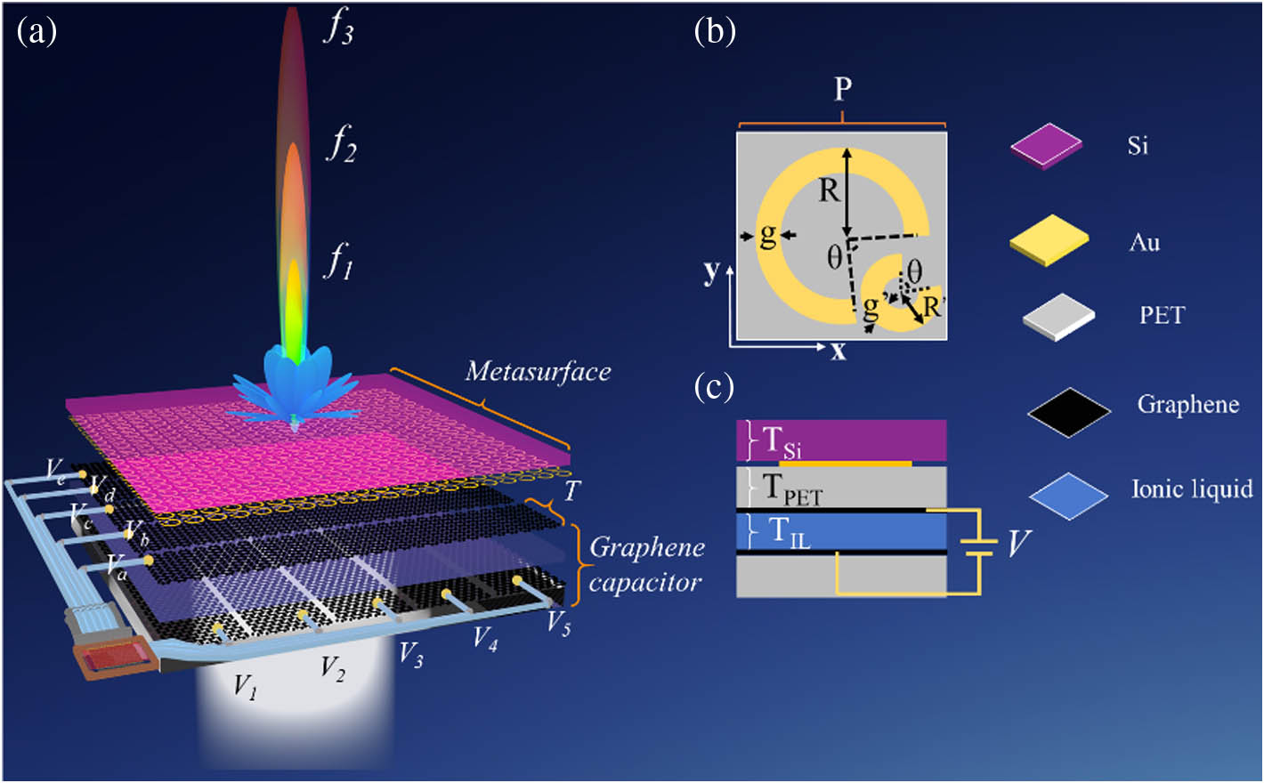
Fig. 1. (a) Schematic of the reconfigurable THz wavefront modulator. The structure consists of a double C-shaped gold antenna array and a 5 × 5 − 75 μm − 45 ° + 45 °
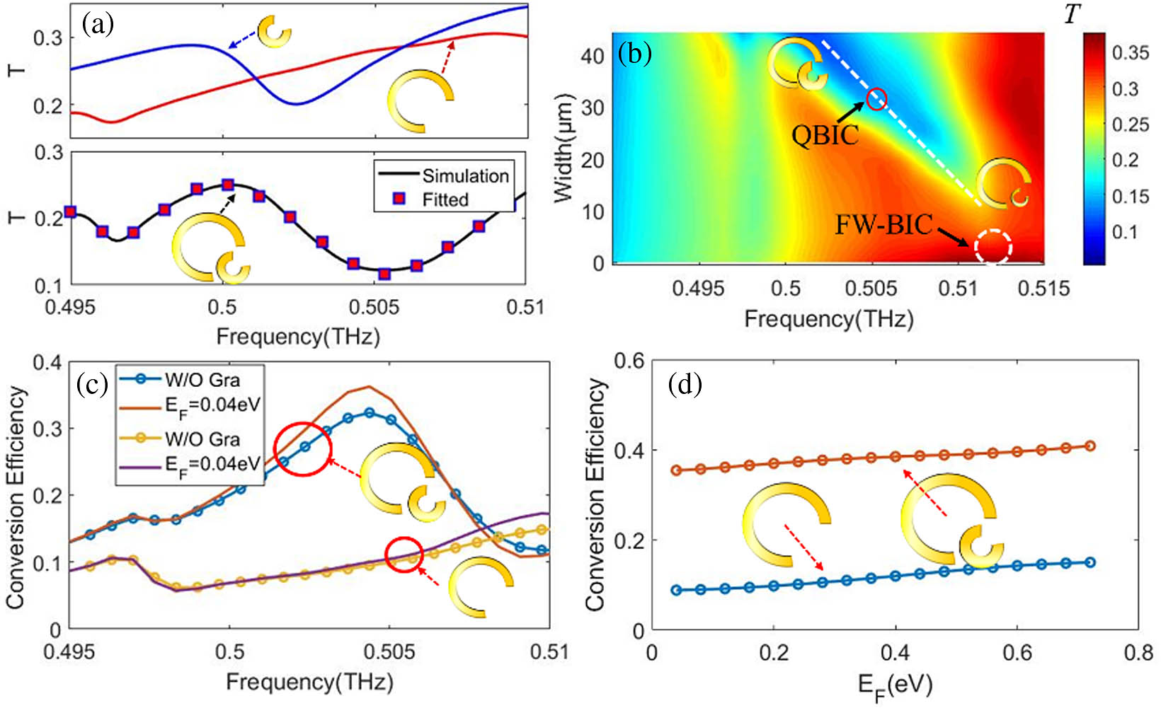
Fig. 2. (a) Simulated transmission spectra of the two individual C-shaped antennas (top) and transmission spectrum of the double C-shaped antenna (bottom). The purple rectangles correspond to the transmissions predicted by the TCMT through fitting the simulated results. (b) Simulated transmission spectrum of the double C-shaped antenna with different outer radii R ′ f = 0.504 THz f = 0.504 THz
Fig. 3. (a)–(c) Illustration of 5 × 5 pixels A ′ , B ′ C ′ x - z
Fig. 4. (a) Schematic of the device fabrication. (b) Fabrication process of the metasurface. (c) Fabrication process of graphene ribbons. (d), (e) Optical image of fabricated metasurface and ablated graphene by laser cutting. (f) Raman spectra of the uncut (red and blue lines) and cut (yellow line) areas.
Fig. 5. (a)–(d) Experimental results of field distribution on the y - z
Fig. 6. (a) Phase spectra of the large C-shaped antenna and small C-shaped antenna in x y Δ φ y = 0.07 π Δ φ x = 0.97 π Q H x f = 0.504 THz f = 0.497 THz | E | f = 0.504 THz y - z y E F = 0.04 eV E F = 0.4 eV E F = 0.56 eV E F = 0.68 eV
Fig. 7. Ablation of graphene under different laser fluences.
Fig. 8. (a) Graphene ribbons after laser cutting. (b) Resistance test of one graphene ribbon. The resistance is 28.9 k Ω
Fig. 9. (a) Fabricated metasurface and graphene ribbons mounted on PCB. (b) Fabricated graphene ribbons connected to PCB by silver paste. (c) THz focal plane imaging system.
Fig. 10. (a), (b) Phase profile obtained by simulation and experiment, respectively. (c) Gate-dependent electrical resistance of graphene on the metasurface. (d)–(f) FWHM and focusing efficiency of modes A, B, and C, respectively.
|
Table 1. Gate Voltages Applied on Graphene

Set citation alerts for the article
Please enter your email address
© Copyright 2018-2021 | Chinese Laser Press. All Rights Reserved 沪ICP备15018463号-20