1Beijing Engineering Research Center for Mixed Reality and Advanced Display, School of Optics and Photonics, Beijing Institute of Technology, Beijing 100081, China
2Beijing Key Laboratory for Metamaterials and Devices, Key Laboratory of Terahertz Optoelectronics, Ministry of Education, and Beijing Advanced Innovation Center for Imaging Technology, Department of Physics, Capital Normal University, Beijing 100048, China
Graphene-based terahertz (THz) metasurfaces combined with metallic antennas have the advantages of ultra-small thickness, electrical tunability, and fast tuning speed. However, their tuning ability is limited by non-independently tunable pixels and low modulation depth due to the ultra-small thickness of graphene. Here, we demonstrate a reconfigurable THz phase modulator with independently tunable units enabled by switching the voltages applied on 10 graphene ribbons prepared by laser cutting. In addition, by introducing quasi-bound states in the continuum resonance through a designed double C-shaped antenna, the efficiency of the device is enhanced by times under different graphene chemical potentials. Experimental results demonstrate that a focus can be formed, and the focal length is changed from 14.3 mm to 22.6 mm. This work provides potential for compact THz spatial light modulators that may be applied in THz communication, detection, and imaging.
1. INTRODUCTION
Terahertz (THz) waves are known as electromagnetic waves located between infrared rays and microwaves, and have attracted much interest in the past few decades [1,2]. Although remarkable progress in THz technology has been made from biomedical science [3], non-destructive detection, and imaging [4] to high-speed wireless communication [5,6], the lack of modulating components, especially wavefront modulators, is one of the major obstacles to the development of THz science and technology [7]. Recently, researchers adopted metasurfaces to solve this problem [8–11]. Because wave modulation can be controlled by designing the geometry of the antennas on the metasurface, such devices have the advantages of light weight, small size, and high design freedom.
However, reconfigurable THz metasurfaces are still highly demanded. Current dynamic metasurfaces for THz wavefront modulation rely on active materials, including electric tuning using liquid crystals [12,13], diodes [6], and 2D materials [14]; thermal tuning using phase change materials [15,16]; and optical tuning using perovskites [17]. Among these tunable devices, active metasurfaces based on graphene have the advantages of fast tuning speed, high transmittance, ultra-small thickness, and good response to THz waves due to the electron intra-band transition, which provides great application potential for THz wavefront control [18–21]. However, the ultra-small atomic thickness of graphene also leads to its weak interaction with a THz wave. Therefore, some attempts combining metallic antennas and monolayer graphene have been proposed [22–24]. Utilizing the strong coupling effect of the metallic structure and THz waves, the modulation depth brought by graphene is also enhanced. Moreover, this kind of composite structure is able to realize tunable phase modulation by geometric design of the antennas [25–28], even though it still faces two problems.
One is lacking independent tuning units. Most of such devices use a complete piece of graphene and apply a uniform gate voltage for tuning; thus, the modulation of each unit cell on the metasurface cannot be changed independently. Although a novel structure endowed with independently tunable pixels was proposed based on graphene ribbons [29], its application in the THz band is hindered by the lack of phase modulation. The other problem is that the interaction between THz waves and this kind of active metasurface is still not high enough. A sandwiched structure for forming a Fabry–Perot cavity has been tried to enhance efficiency [30], whereas the multi-layered structure increases the complexity of the device. It is anticipated that higher efficiency can be achieved using a single metasurface. The reason for the low efficiency is due to the non-radiation ohmic loss and radiation loss [31,32]. Since the inherent dissipation of materials is inevitable, an effective response can be achieved by suppressing the radiation loss [33,34]. Based on this idea, enhancing the metasurface efficiency by the effect of a bound state in the continuum (BIC) has caught researchers’ eyes in recent years.
Sign up for Photonics Research TOC. Get the latest issue of Photonics Research delivered right to you!Sign up now
BICs are localized waves coexisting with a continuous spectrum of radiating waves, which can suppress radiation losses, thus providing a high- effect to enhance the interaction of THz waves with metallic structures [35–38]. In general, there are two types of BICs. One is symmetry-protected (SP) BIC, which results from the complete mode decoupling of different symmetry classes. The other is Friedrich–Wintgen (FW) BIC, caused by the radiation interference of two resonators. By changing the geometric parameters of the resonators, the symmetry of SP-BIC and the radiation interference of FW-BIC is broken and converted to a quasi-BIC (QBIC) mode that can radiate to the external continuum. Therefore, by structure design of metallic antennas to introduce the QBIC mode, the interaction between a single-layered metasurface and a THz wave can be enhanced.
In this paper, we demonstrate an electrically controlled active spatial THz phase modulator with arrays combining 10 graphene ribbons and uniform double C-shaped metallic antennas. Five parallel graphene ribbons are placed perpendicular to the other five, forming graphene capacitors. After attaching the combination of capacitors and metallic antennas to a printed circuit board (PCB), each array can be independently modulated by switching the voltages applied to the graphene ribbons. In addition, by introducing the QBIC from the double C-shaped antennas, the conversion efficiency is enhanced by times under different graphene chemical potentials. Experimental results demonstrate that a focus can be formed and switched to 14.3 mm and 22.6 mm when the applied gate voltages are switched to different modes. At the same time, we use nanosecond-laser-cutting technology to fabricate graphene ribbons from monolayer graphene [39–41]. The minimum linewidth that can be achieved is 25.3 μm. This processing method is suitable for compact tunable THz optical systems and provides a new method for THz communication, detection, and imaging.
2. DESIGN METHOD AND SIMULATION
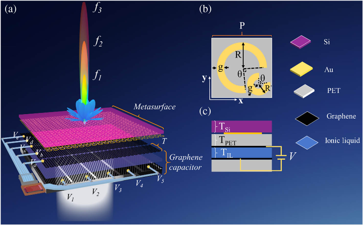
The schematic structure of the reconfigurable THz wavefront modulator is shown in Fig. 1(a), which includes two parts. One is a gold double C-shaped antenna metasurface, while the other is a array of graphene capacitors. The antenna metasurface is fabricated on a high resistance Si substrate () with μ thickness. The whole dimension of the metasurface is , which is composed of identical unit cells. As depicted in Fig. 1(b), each unit cell consists of two C-shaped antennas with the same width (μ), opening angle (), and thickness (), but different sizes. The outer radius of the larger one is μ, and that of the other is μ. The unit cells are squarely arrayed with a period of μ. Since phase modulation is realized through cross-polarized electromagnetic waves excited by gold antennas [11], linearly polarized THz waves (-polarized) are illuminated along the direction, and the transmitted cross-polarized (-polarized) waves are observed.
Figure 1.(a) Schematic of the reconfigurable THz wavefront modulator. The structure consists of a double C-shaped gold antenna array and a array of graphene capacitors composed of 10 graphene ribbons. (b) Top view of one unit cell with the double C-shaped antenna. The centers of the large antenna and small antenna are located at (0 μm,0 μm) and (75 μm, μ), while the opening directions are and , respectively. (c) Side view of the structure.
To realize the phase-tunable effect, a graphene capacitor array is placed close to the antenna metasurface, which consists of two groups of five parallel graphene micro ribbons on polyethylene terephthalate (PET) substrates with a thickness of μ (relative permittivity [42]). The two graphene ribbon groups are orthogonal to each other and separated by an ionic liquid electrolyte (1-butyl-3-methylimidazolium hexafluorophosphate) layer to form a capacitor [29,43], which is shown as the side view of the structure in Fig. 1(c). Thus, when gate voltages and are applied on the top and bottom graphene ribbons separately, as indicated in Fig. 1(a), a built-in electric field array is created, causing various graphene chemical potentials in different square regions, and thereby pixelized electromagnetic responses of the incident THz wave with both the metallic antenna and graphene in these regions are realized. It is worth mentioning that the graphene ribbons have a width of , which means that each pixel of the passive modulator corresponds to metallic unit cells on the metasurface.
To achieve an intense THz–matter interaction, we introduce FW-QBICs through the double C-shaped antenna structure, which can realize Fano resonances with high -factors. The simulation results are conducted by the Lumerical FDTD Solutions software. The resonant responses of two single C-shaped antennas and a double C-shaped antenna in the band of 0.495–0.51 THz are shown in Fig. 2(a). The red (blue) solid line in the top figure denotes the total transmittance of the large (small) single C-shaped antenna and exhibits a resonance at 0.497 THz (0.503 THz) with a transmittance of . By combining the two single C-shaped antennas, it is clearly observed from the black solid line in the bottom figure that the double C-shaped antenna is endowed with a characteristic narrow oscillation of QBIC resonance, and a resonant dip appears at the frequency of . We then employ the temporal coupled mode theory (TCMT) to describe the resonances of the double C-shaped antenna [37,38].
Figure 2.(a) Simulated transmission spectra of the two individual C-shaped antennas (top) and transmission spectrum of the double C-shaped antenna (bottom). The purple rectangles correspond to the transmissions predicted by the TCMT through fitting the simulated results. (b) Simulated transmission spectrum of the double C-shaped antenna with different outer radii of the smaller antenna. (c) Conversion efficiency of the double C-shaped antenna and single C-shaped antenna without graphene and with graphene for . (d) Conversion efficiency of the double C-shaped antenna and single C-shaped antenna versus different graphene chemical potentials for .
The evolution of the two resonant amplitudes in the time domain can be written as [37] where , , , , , , and . is the identity matrix. and are the normalized amplitudes of the two C-shaped antennas. and ( and ) are the normalized amplitudes of incoming (outcoming) waves. is the resonance frequency. is the intrinsic loss, and denotes the radiative loss. is the parity representing the phase difference between the two antennas ( for and for ), and is the kernel parameter that represents the coupling between the modes of the two antennas. Then the transmission can be expressed as where is the total transmission of the silicon and the PET substrates, and . [The phase difference between the two antennas is shown in Fig. 6(a) of Appendix A.] By fitting the simulation results using Eq. (4), we can obtain the parameters of , and . The fitted results are shown as the square dots in Fig. 2(a). It is found that the TCMT perfectly predicts the transmission of the double C-shaped antenna, illustrating that the resonance around 0.505 THz is due to the QBIC mode introduced by the addition of the small C-shaped antenna. The fitted parameters of the resonator system are obtained as follows:
Since BIC appears on the mode with lower radiative loss [44], the fitted parameters confirm the presence of BIC mode at frequency , which corresponds to the resonance of the small C-shaped antenna with higher transmission. Furthermore, the radiative loss is larger than the intrinsic loss ; thus, the transmission feature of a double C-shaped antenna is mainly determined by reflection rather than absorption. This is the reason that it is necessary to design QBIC resonance to suppress radiative loss.
In addition, the proposed double C-shaped antenna can modulate the resonant frequency and -factor by controlling the outer radius of the small antenna, as shown in Fig. 2(b). The QBIC mode can be observed at the white dotted line with the antenna radius ranging from 45 μm to 10 μm. It is found that the spectrum width of the QBIC mode gradually decreases with the decreased antenna width. When the antenna width is less than 10 μm, the transmission dip of QBIC mode gradually disappears, and the QBIC mode becomes the BIC mode, as indicated by the white circle in Fig. 2(b). The conversion behavior demonstrates that this BIC mode is strongly dependent on the optimization of geometric parameters, which is consistent with the characteristics of FW-BIC.
The -factor is an important characteristic of BIC response quality. To quantify the influence of different geometric parameters of the small C-shaped antenna on BIC response quality, the -factors of the QBIC resonance modes are also numerically analyzed as depicted in Appendix A, Fig. 6(b). We also calculated the electric and magnetic field distributions to further understand the resonant mode [see Appendix A, Figs. 6(c) and 6(d), for more analysis].
To better study the contribution of QBIC resonance to the far-field characteristics, we calculated the conversion efficiency [] of both single C-shaped and double C-shaped unit cells, as shown by the circular lines in Fig. 2(c). It can be seen that the conversion efficiency of the single C-shaped antenna corresponding to the yellow circular line slowly increases with the frequency. However, that of the double C-shaped antenna indicated by the blue circular line has two resonant peaks. The conversion efficiency at the dip of 0.497 THz is almost the same as that of the single C-shaped antenna, while the other dip at 0.504 THz [corresponding to the transmission dip of the QBIC resonance in Fig. 2(a)] is 32.3%, which is 3.4 times the 9.5% conversion efficiency of the single C-shaped antenna. The reason for this great efficiency enhancement is that in the QBIC mode, the enhanced local states lead to the reinforcement of interaction between THz wave and the structure, which restrains the transmitted wave with the same polarization while exciting more cross-polarized waves [see Appendix A, Fig. 6(a), for more theoretical analysis]. Furthermore, it is found that the efficiency is still improved by the QBIC when graphene with a chemical potential of 0.04 eV is added to the structure, which is indicated by the red and purple lines in Fig. 2(c). The curves corresponding to the two structures with graphene have variations similar to those without graphene.
Figure 2(d) illustrates the conversion efficiencies of the two structures with a monolayer graphene under various chemical potentials. It is found that the efficiency of the double C-shaped antenna with the introduction of QBIC resonance is greatly improved compared with that of the single C-shaped antenna for all graphene chemical potentials. At 0.04 eV, the conversion efficiency can be improved by 3.6 times, and at 0.68 eV, it can be improved by 2.7 times. Therefore, the interaction between THz waves and the active metasurface can be enhanced by introducing QBIC mode with the double C-shaped antenna.
Moreover, to design a reconfigurable phase modulator of a THz wavefront, dynamic phase modulation is necessary. The phase spectra of transmitted in the band from 0.495 THz to 0.51 THz, corresponding to graphene chemical potentials of , , , and , are plotted in Appendix A, Fig. 6(f).
To realize a pixelized reconfigurable THz wavefront modulator, the phase profile needs to satisfy a certain gradient distribution and can be changed with the graphene chemical potential. Therefore, we designed three chemical potential distributions of graphene corresponding to the required spatial phase modulation, which are denoted by modes , and as shown in Figs. 3(a)–3(c), respectively. The different colored pixels in the checkerboard diagram represent four chemical potentials: , and . Through the design of the specific phase distribution, a focus of the electric field can be realized. At the same time, the focal length can be changed by switching the phase distributions among the three modes of .
Figure 3.(a)–(c) Illustration of of the reconfigurable modulator with three graphene chemical potential distribution modes , and , respectively. The colors represent different graphene chemical potentials. (d)–(f) Simulation results of transmitted amplitude distributions in the plane under the three chemical potential modes.
We verify the tunability of our designed modulator by simulation. The incident light is an -polarized wave with frequency . The distributions of the transmitted electric fields polarized along the axis in the plane, corresponding to modes , and , are depicted in Figs. 3(d)–3(f), respectively. Focuses can be clearly observed under all three modes in both the plane and the focal plane in the inset. Moreover, when the mode changes from to , the focal length increases from to . Therefore, a tuning range of 14.2 mm is obtained, corresponding to .
3. FABRICATION AND EXPERIMENT RESULT
To demonstrate the versatility of our approach, we fabricated the device and measured its performance of active modulation. Figures 4(a)–4(c) show the fabrication process of the designed reconfigurable THz wavefront modulator. As introduced in Fig. 1, the device shown in Fig. 4(a) is mainly composed of a double C-shaped metallic metasurface and a graphene capacitor. The fabrication of the metasurface component is demonstrated in Fig. 4(b). We first prepared a high-resistance silicon substrate with a size of and thickness of 500 μm. A layer of S1813 photoresist was spin-coated on the silicon wafer at a speed of 500 r/min for 6 s, followed by 3000 r/min for 30 s. Then it was dried at 110°C for 90 s. Second, a UV lithography system produced the pattern on the photoresist under a Cr-plated quartz mask. In the third step, we deposited a 10 nm Cr layer and a 90 nm gold layer onto the photoresist by electron beam evaporation coating technology. The Cr layer acted as an adhesive. The vacuum pressure was (), and the deposition rate was 0.5 Å/s (1 Å = 0.1 nm). Finally, the double C-shaped array was obtained by passing a lift-off process. Figure 4(d) shows the photograph of the antenna array after fabrication under a metalloscope (MGL6000).
Figure 4.(a) Schematic of the device fabrication. (b) Fabrication process of the metasurface. (c) Fabrication process of graphene ribbons. (d), (e) Optical image of fabricated metasurface and ablated graphene by laser cutting. (f) Raman spectra of the uncut (red and blue lines) and cut (yellow line) areas.
The graphene capacitor was prepared as shown in Fig. 4(c). First, two monolayers of graphene synthesized by chemical vapor deposition (CVD) technology prepared on copper foils were transferred onto a flexible 200 μm thick PET substrate. Then a 532 nm laser beam generated by a nanosecond solid-state laser (Changchun New Industries Optoelectronics Tech. Co., Ltd.), with a spot diameter of 5 μm and a pulse width of 150 ns, was focused by a telecentric scan lens with a focal length of 60 mm and a matching scanning system with a scanning speed of 60 mm/s on the graphene film. The selection of the laser fluence is described in Fig. 7 of Appendix B. The matching scanning system is linked to a computer and thus can control the laser focus precisely. Two graphene sheets () were evenly cut into five rectangular ribbons with a period of 0.24 cm. We used a multimeter to test the electrical isolation of graphene ribbons after laser cutting. (The conductive performance of graphene ribbons is shown in Fig. 8 of Appendix C.) After the metasurface and graphene ribbons were fabricated, a paper tissue with a thickness of μ was used as a spacer between the two perpendicularly placed arrays of graphene ribbons. Then we used a burette to slowly soak the ionic liquid (1-butyl-3-methylimidazolium hexafluorophosphate) into the paper tissue and make it disperse between the graphene ribbons. Finally, the metasurface was placed on the graphene capacitor, as shown in Fig. 4(a).
The ablated regions on graphene by the laser fluence as are also characterized by the metalloscope. In Fig. 4(e), the dark area marked by point 2 corresponds to the cut region, while the bright areas marked by points 1 and 3 are uncut regions. It is measured that the width of the ablation area is 28.6 μm, which is larger than the laser beam spot size of 5 μm. The reason relies on the heating effect of the laser pulse, which influences a larger area than the spot size. This effect is also seen by the bright edges on both sides of the ablated region, which indicates the melt PET substrate caused by the nanosecond laser heating. More clean edges can be obtained by using femtosecond laser cutting or the lithography process [40]. However, the bright melt PET substrate is only μ wide, which is negligible compared to the unit cells.
To further illustrate the characteristics of the cut and uncut graphene areas, Raman spectra of the marked points are shown in Fig. 4(f) (Renishaw RM2000). It can be found that the D peak () is almost unobservable, while the graphitic G peak () and 2D peak () show strong intensities in the uncut area. In contrast, due to the removal of both the PET substrate and graphene in the ablation area, the Raman spectrum of the cut region does not show the characteristic peaks.
We then designed and fabricated a PCB to apply voltage independently on the 10 graphene ribbons. The fabricated device mounted on the PCB and the THz imaging system is demonstrated in Fig. 9(a) of Appendix D. The graphene ribbons were connected by conductive silver paste to 10 electrodes on the PCB. [Photographs of the graphene capacitor and electrodes are shown in Figs. 9(b) and 9(c) of Appendix D.] A THz focal plane imaging system was used to obtain the near-field complex amplitude distribution [27].
Figure 5.(a)–(d) Experimental results of field distribution on the plane when the voltages are applied in four modes: A, B, C, and D. The intensities are normalized by the maximum intensity of mode B. (e) Broadband performance of the device. (f) Relationship between the applied gate voltage and graphene chemical potential.
The measured THz field distributions under the four voltage modes are shown in Figs. 5(a)–5(d). The focusing effect can be observed in Figs. 5(a)–5(c) corresponding to modes A–C. The insets show the focus on the focal planes. Figure 5(d) demonstrates the measured THz field distribution of mode D, in which no gate voltage is applied. There is no focus observed in the figure, indicating that the phase of the transmitted THz wavefront is not modulated without applying the voltage. A tunable focal length is achieved when the voltages applied on the graphene ribbons are varied. The focal length is , and when the gate voltages are applied in modes A–C, respectively. The focal length is changed by 8.3 mm (). These experimental results show that dynamic phase modulation of THz waves is achieved by the proposed device.
The broadband performance of the device was also measured, which is illustrated in Fig. 5(e). The focal length variation exceeds 4.55 mm in the band from 0.44 to 0.68 THz when the gate changes from mode A to C. However, when the frequency is above 0.97 THz or below 0.32 THz, the focal length changes by less than 0.42 mm. The reason for the narrow modulation bandwidth (0.24 THz) is that the antenna array is designed based on QBIC resonance, which is characterized by high -factors but has a narrow spectrum bandwidth. The focal length variation in the experiment (8.3 mm) is different from that in the simulation (14.2 mm) because there are fabrication errors in the gap distance between different layers when the modulator is installed on the printed circuit board (PCB). To further discuss the focusing of the modulator, we calculate the full width at half maximum (FWHM) and focusing efficiency of the focus obtained in the experiment as shown in Figs. 10(d)–10(f) in Appendix E.
The graphene carrier density can be calculated when the gate voltage is applied. At the same time, the relationship between the applied gate voltage and the chemical potential of graphene is obtained, as shown in Fig. 5(f) [24]. The charge-neutral Dirac point of the graphene is found when the applied voltage is by measuring the resistance of graphene versus the applied voltage, as shown in Fig. 10(c) of Appendix E. The estimated thickness of the air gap between the ionic liquid and the graphene layer is 0.5 nm.
4. CONCLUSION
In summary, we propose a BICs-enhanced active THz modulator enabled by laser-cut graphene ribbons. Both the flexible manipulation of the phase profile and enhancement of conversion efficiency are realized in the THz band based on this modulator. By introducing the QBIC mode, the conversion efficiency is enhanced by times. Thus, a THz modulator based on a matrix array that can be independently modulated by switching the voltages applied on 10 graphene ribbons is designed and experimentally demonstrated. It is experimentally demonstrated that the modulator can switch between focusing lenses and a plane lens, and the focal length can be shifted by . Also, we used laser-cutting technology to fabricate graphene ribbons, which is suitable for compact tunable THz optical systems. We anticipate that the proposed THz modulator can provide an effective strategy to flexibly manipulate THz waves and can be applied to THz communication, detection, and imaging.
APPENDIX A: THEORETICAL ANALYSIS OF THE BIC MODEL
To determine the parity and to understand the response mechanism more deeply, we demonstrate the phase spectra of the two C-shaped antennas in and polarization directions, as shown in Fig. 6(a). It can be seen that the phase difference between the two C-shaped antennas in direction and direction is quite different ( and , respectively); thus, destructive interference occurs in polarization and constructive interference occurs in the cross polarization. This is also the theoretical reason for the enhanced conversion efficiency shown in Figs. 2(c) and 2(d). The introduced QBIC model puts the -polarized electric field component in a bound state and enhances the interaction between the THz wave and the modulator, resulting in excitation of more cross-polarized electric field components and constructive interference of the cross-polarized electric fields excited by the two C-shaped antennas, thus achieving efficiency enhancement as shown in Fig. 2.
Figure 6.(a) Phase spectra of the large C-shaped antenna and small C-shaped antenna in and polarizations ( and ). (b) Relation between the -factor of QBIC and the width of the small C-shaped antenna. (c), (d) Instantaneous directions of surface magnetic field () and their distributions at frequencies of and , respectively. The gray dotted line denotes the outline of the gold antennas (top view). (e) Instantaneous directions and absolute value distribution of the electric field () at the frequency of in the plane (side view). (f) Phase spectra of transmitted -polarized wave corresponding to , , , and .
Figure 6(b) shows the relation between the -factor and the width () of the small C-shaped antenna. The -factor can be calculated as the ratio of the resonant frequency () to its FWHM () and written as [34]. It can be seen that the value increases with the decrease in width, and diverges when the width approaches 0 μm, which is also a common signature of BIC modes [46]. The width is selected as 30 μm in our design to excite QBIC mode, indicated by the red circle in Fig. 2(b), which is a comprehensive consideration including a sufficient -factor (the corresponding -factor for this width is 84) and possible realizations in both simulation and fabrication.
To further confirm that resonance is caused by QBIC, the distributions of magnetic field component excited by the double C-shaped metallic antenna at frequencies of and are calculated and shown in Figs. 6(c) and 6(d), respectively. The red and blue colors represent the positive and negative magnetic fields, respectively, and the gray dotted line denotes the outline of the two antennas. It is observed from Fig. 6(c) that there are two strong magnetic dipoles ( and modes) for the large antenna and small antenna, respectively. The MD corresponding to resonance is mainly concentrated on the left part of the large C-shaped antenna, while that corresponding to resonance is evenly distributed on the small C-shaped antenna. In contrast to SP-BICs, the MDs excited by the double C-shaped antenna have no symmetry in the plane. Figure 2(a) demonstrates that the introduction of the QBIC mechanism at the frequency of is mainly due to the addition of the small C-shaped antenna. Therefore, when the incident frequency is changed to , it can be seen from Fig. 6(d) that the MD resonant mode on the small C-shaped antenna is very weak, and thus, QBIC resonance is not excited. This is why the conversion efficiency in Fig. 2(c) increases when the frequency is changed from to .
To have a deeper insight into the MD resonant modes, we also plot the instantaneous directions of the magnetic field at frequencies of and in Figs. 6(c) and 6(d), which are represented by black arrows. Counterclockwise and clockwise red dotted arrows represent and resonant modes, respectively. The two resonant modes radiate into the same transmitted field; thus, radiation interference excites the FW-BIC mode. Figure 6(e) shows the distribution of in the plane corresponding to the position indicated by the white line in Fig. 6(c). The white arrows represent the instantaneous direction of the electric field, and the red dotted line indicates the direction of the electric field excited by the clockwise magnetic field. FW-BIC results from the interference of the two resonators’ radiation.
Figure 6(f) shows the phase shift with different chemical potentials. The phase spectrum is continuously shifted as the graphene chemical potential increases from 0.04 eV to 0.68 eV, which suggests that dynamic phase modulation can be achieved. The maximum phase change () is at 0.507 THz, which indicates that a reconfigurable phase modulator of the THz wavefront is able to be designed.
APPENDIX B: LASER PARAMETER SELECTION
To determine the optimal laser parameters for the graphene cut, we experimentally tested the influence of different laser fluences on the morphology of the cut graphene. The pulse width and scanning speed of the laser are set as 150 ns and 60 mm/s, respectively. Figures 7(a)–7(d) show the metalloscope images of the corresponding surface morphologies of the cut area when the laser fluence is , , , and , respectively. A higher laser fluence means stronger laser power. Thus, it can be seen clearly in Figs. 7(a) and 7(b) that with the increase of the laser fluence, the ablation area becomes more and more obvious. When the laser fluence is larger than , the ablation region becomes black, which means the laser not only ablates the graphene and the PET substrate, but also carbonizes them at high temperatures during cutting. The high temperature brought by the high-power laser pulse makes the cutting edge very uneven, and the linewidth increases with laser power. When the laser fluence decreases from to , the linewidth of the cutting channel decreases from 72.2 μm to 30.2 μm, and the carbonization of the cutting area becomes weaker, as shown in Fig. 7(c). Figure 7(d) shows the cutting limit we can reach. When the laser fluence is , not only a clean cutting edge without carbonization can be obtained, but also the cutting region linewidth can be realized as small as 25.3 μm. If the laser fluence is lower than , the ablated area is not visible in the microscope. Therefore, as shown in Fig. 4(e), we chose the laser fluence as to prepare the graphene ribbons. This is because although the channel with a cleaner edge and smaller linewidth is processed in Fig. 7(d), it is too small to be observed by the naked eye; thus, it is not convenient to use silver paste to connect the graphene ribbons to the electrodes on the PCB when processing wire-bonding.
Figure 7.Ablation of graphene under different laser fluences.
APPENDIX C: ELECTRICAL CONDUCTIVITY BETWEEN GRAPHENE RIBBONS
To achieve independent modulation of different pixels, each graphene ribbon must be electrically isolated from the other. Figure 8(a) shows our processed graphene layers, which are in size. We used a multimeter to determine the conductive performance of each graphene ribbon and that between different ribbons. Figures 8(b) and 8(c) demonstrate that two adjacent graphene ribbons are electrically isolated after laser cutting, while the resistance of the graphene ribbon is .
Figure 8.(a) Graphene ribbons after laser cutting. (b) Resistance test of one graphene ribbon. The resistance is . (c) Resistance test of adjacent graphene ribbons demonstrating electrical isolation.
APPENDIX D: FABRICATED PRINTED CIRCUIT BOARD AND THE THz IMAGING SYSTEM
The fabricated device mounted on the PCB is shown in Fig. 9(a). The red dotted line indicates the position of the metasurface, and the antenna array is on the back. Below the metasurface is the graphene capacitor, as shown in Fig. 9(b). We connect the graphene ribbons with the PCB electrodes using silver paste, as shown in the blue oval. Figure 9(c) shows the THz imaging system. The three circuit boards in the red box are multi-channel power supplies that provide independent voltages to the 10 graphene ribbons.
Figure 9.(a) Fabricated metasurface and graphene ribbons mounted on PCB. (b) Fabricated graphene ribbons connected to PCB by silver paste. (c) THz focal plane imaging system.
To compare the near-field results obtained by experimental detection and simulation results, Figs. 10(a) and 10(b) show the near-field phase profile cross sections obtained by simulation and experiment, respectively. The red, blue, and yellow curves correspond to modes A, B, and C in Fig. 3, respectively. The distance between the probe crystal and the device is about 2 mm, and the distance between the monitor and the transmitted plane in the simulation is also set as 2 mm. The position of the charge-neutral Dirac point of graphene is found by changing the applied voltage to measure the resistance of the graphene on the sample, as shown in Fig. 10(c). The Dirac point corresponding to the maximum resistance occurs at . This is because there is no charge transfer between the PET substrate and graphene, and thus, the graphene is undoped.
Figure 10.(a), (b) Phase profile obtained by simulation and experiment, respectively. (c) Gate-dependent electrical resistance of graphene on the metasurface. (d)–(f) FWHM and focusing efficiency of modes A, B, and C, respectively.
To analyze the focusing of our modulator, Figs. 10(d)–10(f) show the cross sections of the focal plane in the experiment. We calculate the FWHMs as , and corresponding to voltage application modes A, B, and C, respectively. The ideal diffraction limits are calculated as , and , respectively, which shows that the experimental focus is larger than the ideal diffraction limit [47]. Thus, this modulator is a diffraction-limited device due to an insufficient pixel count. We also calculated the focusing efficiency () based on the experiment results, defined as the ratio of the energy in an area with a radius three times the FWHM to the energy of incident light [48]. In modes A, B, and C, the focusing efficiencies are 1.2%, 11.5% and 1.32%, respectively. The reason for the lower efficiency in modes A and C is that the voltage () applied in modes A and C is larger than that applied in mode B, resulting in a higher chemical potential of graphene and leading to the increase in ohmic loss and the screening of THz waves [49].
[18] A. Zaman, N. W. Almond, Y. Lu, X. Romain, D. A. De Lima, H. Lin, O. Burton, J. Alexander-Webber, S. Hofmann, T. Mitchell, J. D. P. Griffiths, H. E. Beere, D. A. Ritchie, R. Degl’Innocenti. Graphene-based external optoelectronic terahertz modulators for high speed wireless communications. 14th UK-Europe-China Workshop on Millimetre-Waves and Terahertz Technologies (UCMMT), 1-3(2021).
[42] Y. Ohki, N. Fuse, S. Hikosaka, Y. Takemura, M. Mizuno, K. Fukunaga. Complex permittivity spectra of several insulating polymers at electrical and THz frequencies. 2009 IEEE Conference on Electrical Insulation and Dielectric Phenomena, 7-10(2009).