• Acta Optica Sinica
  • Vol. 41, Issue 9, 0913002 (2021)
Xueting Han1、2, Hongming Fei1、2、*, Han Lin3, Yibiao Yang1、2, Binzhao Cao1、2, Mingda Zhang1、2, Yuan Tian1、2, and Wenqiang Zhi1、2
Author Affiliations
  • 1Department of Physics and Optoelectronics, Taiyuan University of Technology, Taiyuan, Shanxi 0 30024, China
  • 2Key Laboratory of Advanced Transducers and Intelligent Control System, Ministry of Education, Taiyuan University of Technology, Taiyuan, Shanxi 0 30024, China
  • 3Centre for Translational Atomaterials, Swinburne University of Technology, Victoria 3122, Australia
  • show less
    DOI: 10.3788/AOS202141.0913002 Cite this Article Set citation alerts
    Xueting Han, Hongming Fei, Han Lin, Yibiao Yang, Binzhao Cao, Mingda Zhang, Yuan Tian, Wenqiang Zhi. Design of Optical Waveguide Heterostructure with Fully Photonic Bandgap for Asymmetric Transmission of Circularly Polarized Light[J]. Acta Optica Sinica, 2021, 41(9): 0913002 Copy Citation Text show less
    Structural diagram of two-dimensional photonic crystal waveguide heterostructure, and refractive index distribution of substrate material along x-direction position. (a) Structural diagram of two-dimensional photonic crystal waveguide heterostructure; (b) refractive index distribution of substrate material along x-direction position
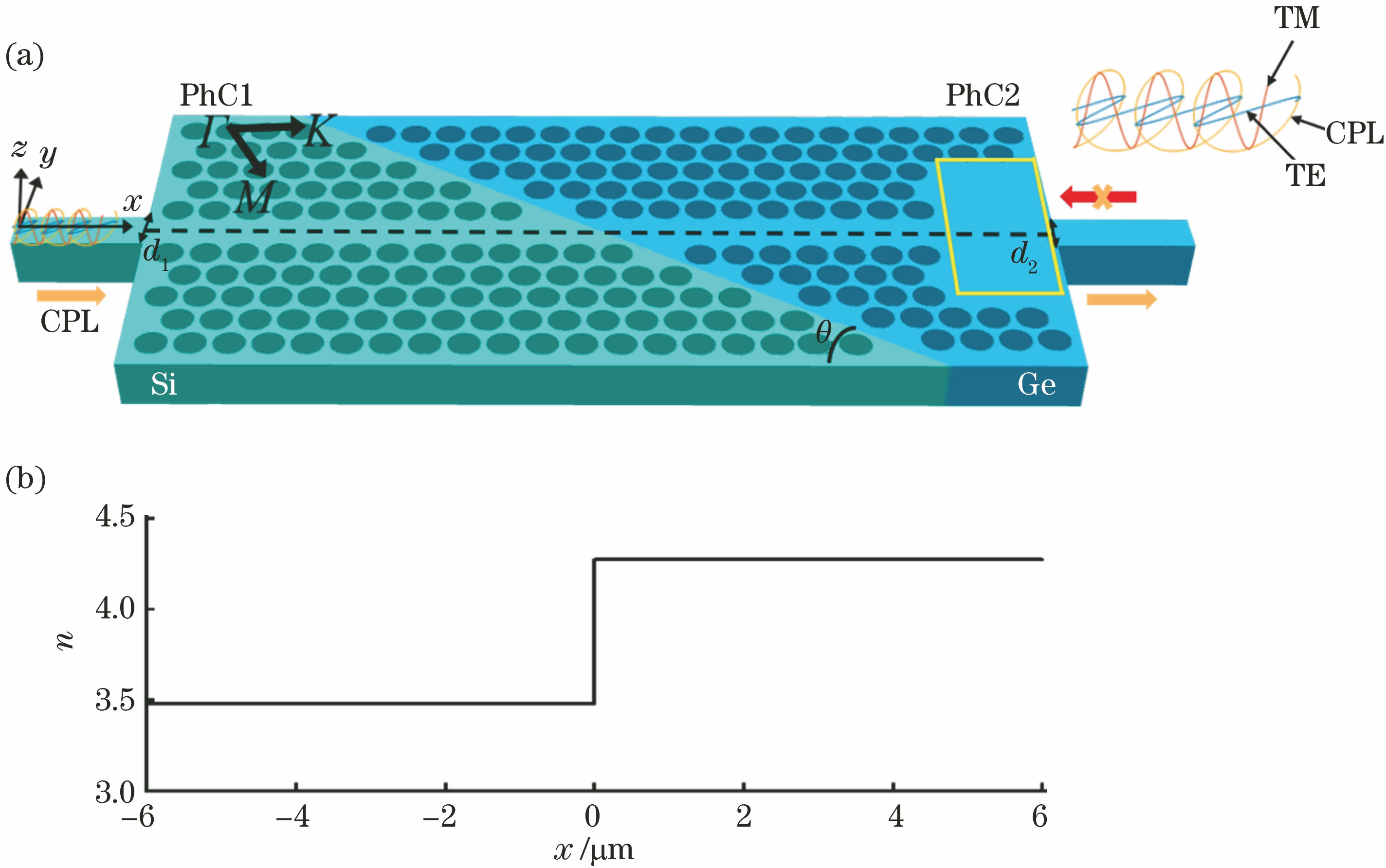
    Fig. 1. Structural diagram of two-dimensional photonic crystal waveguide heterostructure, and refractive index distribution of substrate material along x-direction position. (a) Structural diagram of two-dimensional photonic crystal waveguide heterostructure; (b) refractive index distribution of substrate material along x-direction position
    TE and TM energy band diagrams of PhC1 and PhC2, and photonic bandgaps of TE and TM modes of PhC1(PhC2) varying with r1(r2). (a) TE and TM energy band diagrams of PhC1; (b) TE and TM energy band diagrams of PhC2; (c) photonic bandgaps of TE and TM modes of PhC1 varying with r1; (d) photonic bandgaps of TE and TM modes of PhC2 varying with r2
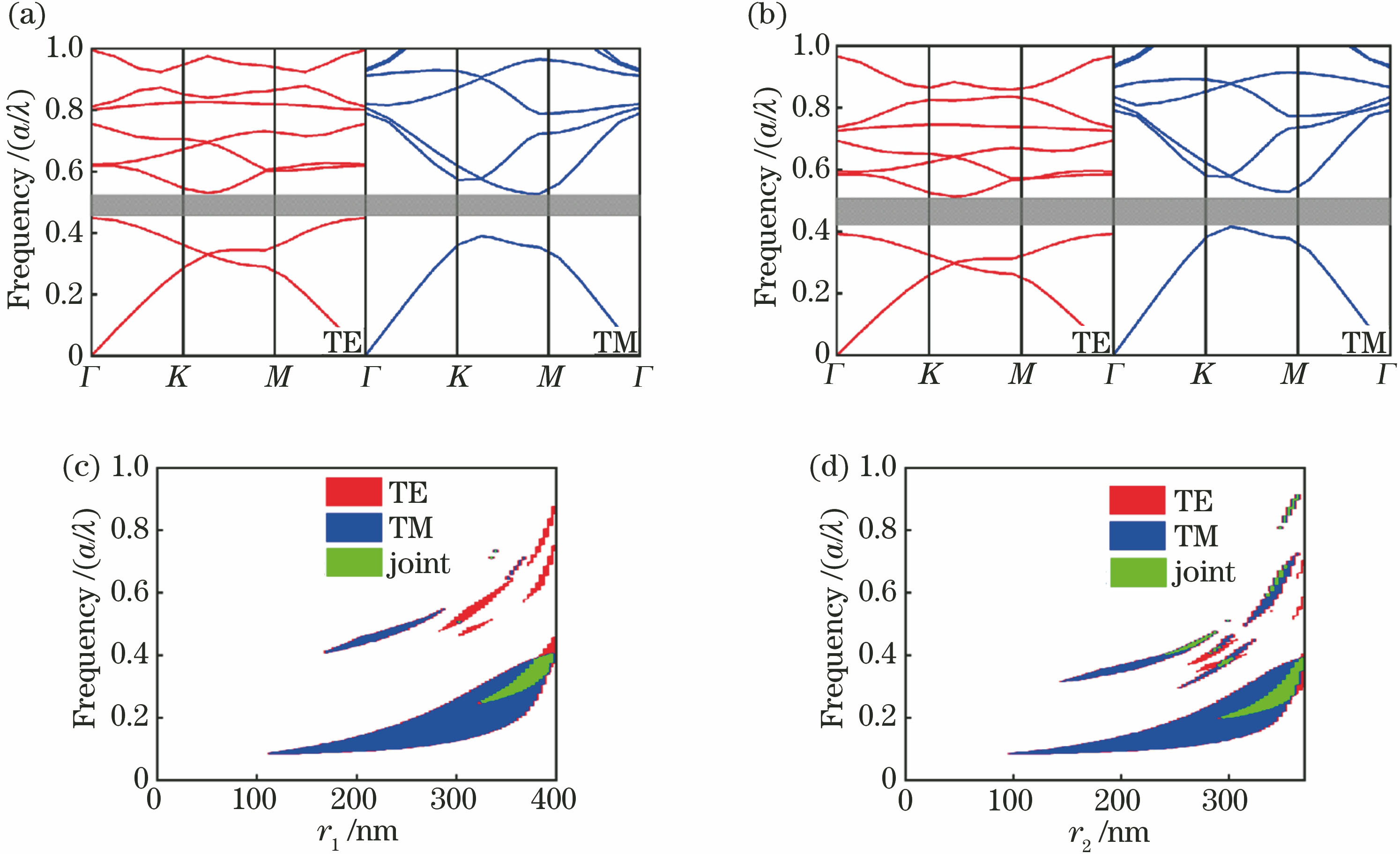
    Fig. 2. TE and TM energy band diagrams of PhC1 and PhC2, and photonic bandgaps of TE and TM modes of PhC1(PhC2) varying with r1(r2). (a) TE and TM energy band diagrams of PhC1; (b) TE and TM energy band diagrams of PhC2; (c) photonic bandgaps of TE and TM modes of PhC1 varying with r1; (d) photonic bandgaps of TE and TM modes of PhC2 varying with r2
    Transmittance of TE, TM, and CPL in PhC1 and PhC2 as a function of width of waveguide. (a)-(c) Transmittance of TE, TM, and CPL in PhC1 as a function of d1 for step of 20 nm; (d)-(f) transmittance of TE, TM, and CPL at 1550 nm in PhC1 for different d1; (g)-(i) transmittance of TE, TM, and CPL in PhC2 as a function of d2 for step of 20 nm; (j)-(l) transmittance of TE, TM, and CPL at 1550 nm in PhC2 for different d2
    Fig. 3. Transmittance of TE, TM, and CPL in PhC1 and PhC2 as a function of width of waveguide. (a)-(c) Transmittance of TE, TM, and CPL in PhC1 as a function of d1 for step of 20 nm; (d)-(f) transmittance of TE, TM, and CPL at 1550 nm in PhC1 for different d1; (g)-(i) transmittance of TE, TM, and CPL in PhC2 as a function of d2 for step of 20 nm; (j)-(l) transmittance of TE, TM, and CPL at 1550 nm in PhC2 for different d2
    Forward and backward incident electric field intensity distributions at 1550 nm of heterostructure after removing 6×3 air holes on right side of PhC2. (a) TE, forward; (b) TM, forward; (c) CPL, forward; (d) TE, backward; (e) TM, backward; (f) CPL, backward; transmittance spectra of studied waveband of (g) TE, (h) TM, and (i) CPL
    Fig. 4. Forward and backward incident electric field intensity distributions at 1550 nm of heterostructure after removing 6×3 air holes on right side of PhC2. (a) TE, forward; (b) TM, forward; (c) CPL, forward; (d) TE, backward; (e) TM, backward; (f) CPL, backward; transmittance spectra of studied waveband of (g) TE, (h) TM, and (i) CPL
    Electric field intensity, polarization, and phase distributions of CPL in y-z plane of 2D PhC heterostructure, transmittance and transmittance contrast of CPL in 2D PhC heterostructure, and forward transmittance of CPL in 2D PhC structure and finite thickness PhC heterostructure slab based on silica substrate. (a) Electric field intensity,polarization distribution, and (b) phase distribution of CPL in y-z plane of 2D PhC heterostructure; (c) transmittance and transmittance contrast of CPL in 2D PhC heterostructure; (d) forward transmittance of CPL in 2D PhC structure and finite thickness PhC heterostructure slab based on silica substrate
    Fig. 5. Electric field intensity, polarization, and phase distributions of CPL in y-z plane of 2D PhC heterostructure, transmittance and transmittance contrast of CPL in 2D PhC heterostructure, and forward transmittance of CPL in 2D PhC structure and finite thickness PhC heterostructure slab based on silica substrate. (a) Electric field intensity,polarization distribution, and (b) phase distribution of CPL in y-z plane of 2D PhC heterostructure; (c) transmittance and transmittance contrast of CPL in 2D PhC heterostructure; (d) forward transmittance of CPL in 2D PhC structure and finite thickness PhC heterostructure slab based on silica substrate
    Xueting Han, Hongming Fei, Han Lin, Yibiao Yang, Binzhao Cao, Mingda Zhang, Yuan Tian, Wenqiang Zhi. Design of Optical Waveguide Heterostructure with Fully Photonic Bandgap for Asymmetric Transmission of Circularly Polarized Light[J]. Acta Optica Sinica, 2021, 41(9): 0913002
    Download Citation