Qi Sun, Przemyslaw Falak, Tom Vettenburg, Timothy Lee, David B. Phillips, Gilberto Brambilla, Martynas Beresna, "Compact nano-void spectrometer based on a stable engineered scattering system," Photonics Res. 10, 2328 (2022)
Copy Citation Text
Random scattering of light in disordered media can be used for highly sensitive speckle-based wavemeters and spectrometers. However, the multiple scattering events that fold long optical paths within a compact space also make such devices exceedingly sensitive to vibrations and small disturbances to the disordered media. Here, we show how scattering can be engineered so that it can be used for a compact computational spectrometer that is largely insensitive to environmental factors. We designed and fabricated a three-dimensional pseudo-random nano-void pattern with 62% scattering efficiency. The controlled amount of multiple scattering ensured a sufficiently long optical path for the target resolution of 100 pm, with optimal long-term stability. The 200-μm-thick scattering silica substrate was integrated in a compact assembly with a low-cost camera sensor. The target resolution was achieved for full spectrum measurements while single wavelengths could be determined with 50 pm resolution. Such tailored scattering systems can improve the trade-off among cost, size, stability, and spectral resolution in computational spectrometers.
1. INTRODUCTION
Accurate wavelength measurement is central for analysis and characterization in various disciplines, including biology, chemistry, material analysis, and astronomy. The conventional approach for extracting spectral information relies on a diffraction grating to separate the spectral components. A key parameter for such a system is the optical path length between the dispersive element and the detector. Fine spectral resolution requires a large optical path length and correspondingly a large instrument footprint.
An alternative method is to exploit the dispersion inherent in multiple cascaded light scattering events to implement spatial mapping of spectral components [1,2]. Multiple scattering would increase the equivalent optical path of light, beyond the actual physical size of the system [3,4]. Therefore, a small shift in the wavelength of input light can result in a large change in its generated speckle pattern. Many approaches for implementing scattering media have been exploited: multimode fiber, integrating spheres, alumina powder, and 2D scattering chips. These have all provided a high spectral resolution, yet a key challenge remains unsolved: the mechanical stability of the scattering sample itself. Here we propose a 3D scattering chip made of material with intrinsic environmental (thermal and mechanical) stability and inscribed with densely packed laser-written nano-voids. These arrays of scattering centers create a high degree of spectral dispersion within a small volume, effectively folding the optical path. As a result, multiple scattering events produce intricate speckles that are highly wavelength dependent [5]. Despite their random appearance, such patterns are deterministic provided that the scattering element is static in nature.
Scattering spectrometers have been demonstrated using several different scattering elements. A multimode-fiber-based system reaching a fine resolution of 1 pm was demonstrated using 100 m of fiber waveguide [6], where the speckle pattern is formed by interference of many higher-order modes. The resolution in this arrangement is proportional to the length of the fiber. To achieve a 0.1 nm resolution, a length of at least 1 m of fiber () is required [7]. Unfortunately, the longer waveguide also makes it sensitive to small environmental perturbations and vibrations, thus rendering it impractical for many applications. Such systems require regular re-calibration and must remain unchanged after the calibration for each test [8]. Wavemeters based on an integrating sphere have been used to demonstrate sub-femtometer resolution [9,10], yet size and stability requirements limit applications to specialist and laboratory settings. Since 2013, a compact spectrometer chip based on a silicon-on-insulator scattering medium has been utilized to increase the optical path length and enable better spectral resolution within the same physical space. The first version of such a device was designed as two-dimensional random air holes etched into the silicon plane [5]. It had a resolution of 0.75 nm at a wavelength of 1500 nm in a 25-mm-radius structure. However, as the scattering medium was designed in a single plane, the chip could operate only with limited detectors, thus limiting wavelength channels in two dimensions. Soon after, a wavelength meter using alumina () powder (3D approach) was demonstrated [11]. By analyzing the intensity pattern created by multiple scattering within a dried drop of alumina, the illumination wavelength could be determined with 13 pm accuracy. However, the instability of alumina powder renders performance extremely sensitive to vibrations and alignment drift. Because of this, interest was refocused on chip-based systems. As a result, the chip strategy evolved, either by miniaturization, increasing number of output ports, or expanding the structure from 2D to 3D (multiple planes approach) [12–14]. Transition into 3D design enabled key advantages: applying 3D detector arrays (more detection channels) and generating more sophisticated speckle patterns (cascaded scattering events), which increased the optical resolution of such devices. Nowadays, chip-based spectrometers can achieve single-photon sensitivity [15], yet still the main challenge persists: the stability of both the scattering medium and the device itself. More generally, while such highly scattering dispersive systems offer greater potential resolution, the practical resolution will be stability limited by its higher environmental sensitivity [16]. It is therefore important to maximize stability while adapting the level of scattering to optimally match the required spectral resolution for the application.
Sign up for Photonics Research TOC. Get the latest issue of Photonics Research delivered right to you!Sign up now
Here, we demonstrate a highly stable, low-cost, compact, and high-resolution spectrometer. To minimize the influence of vibrations and thermal gradients, our design is based on a single monolithic block of silica. We first describe how femtosecond laser direct writing can be used to create a pseudo-random distribution of nano-voids that scatter light in a wavelength dependent manner, tunable by design. The following sections discuss the calibration and characterization of its high-stability operation.
2. PSEUDO-RANDOM SCATTERING SPECTROMETER
A. Nano-Void Scattering Chip
We designed a planar pattern of pseudo-random scattering nano-voids that can be readily produced using direct laser writing. Femtosecond lasers can generate nano-voids with sub-microjoule pulse energies [17]. The highly non-linear interaction of femtosecond pulses with the transparent substrate enables the formation of densely packed spherical cavities without collateral damage. We exploit this to produce a pseudo-random geometry with an average void separation of 1 μm.
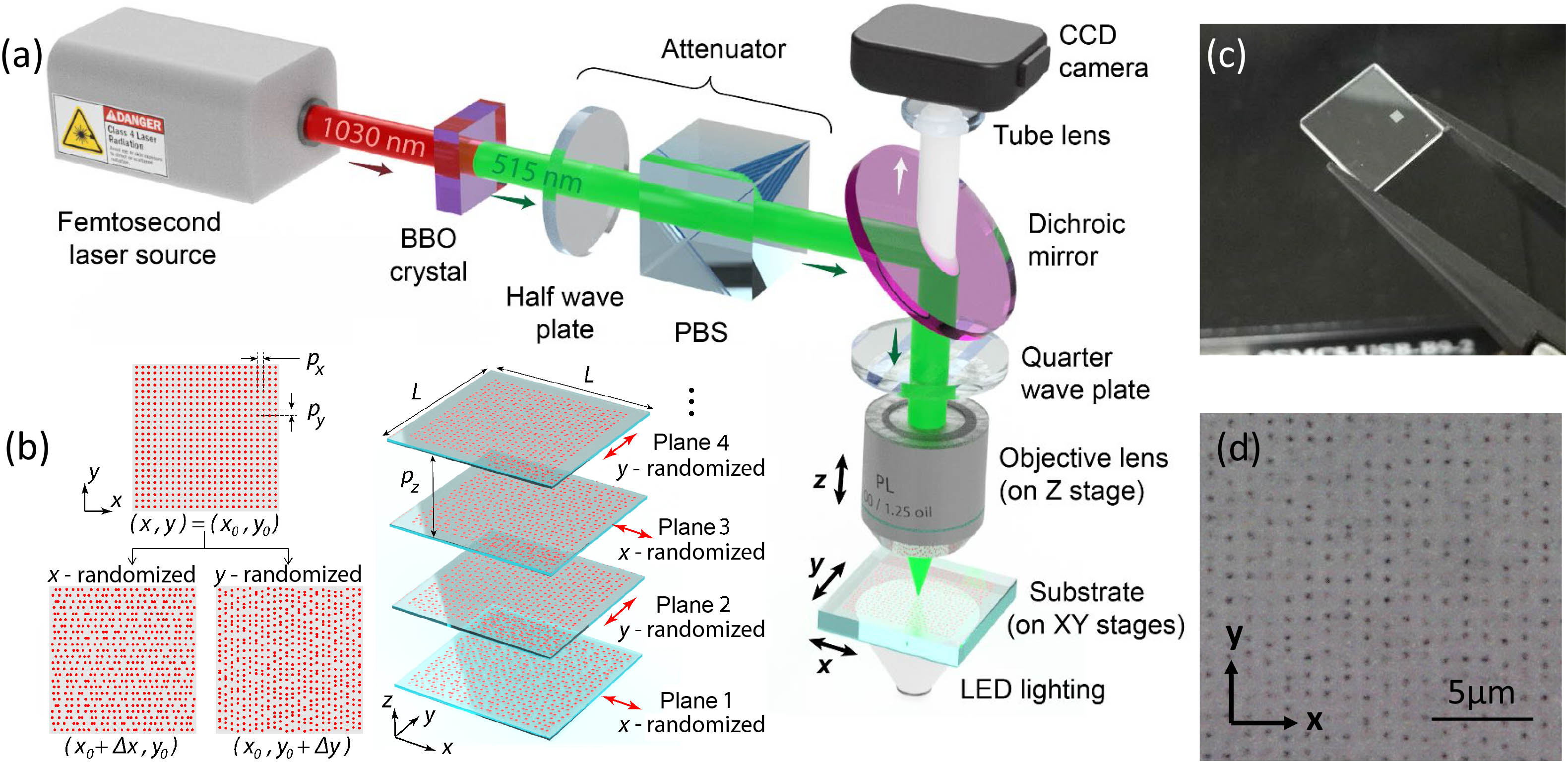
Figure 1(a) shows a schematic of the optical system used for writing the custom scattering chip. Micro-cavities are formed using a femtosecond laser (Pharos, Light Conversion Ltd., Lithuania) with central wavelength of μ, pulse duration of , and repetition rate of . To enhance the writing resolution, we used the second harmonic for laser writing. A computer controlled translation stage was used to translate the silica substrate with respect to the beam in horizontal directions and , while the height of the oil-immersion objective (NA 1.25) was adjusted in the vertical direction. The overhead CMOS camera allowed in situ visualization of the writing process and the initial quality inspection of the imprinted structures. Each void was produced by a single pulse of energy 220 nJ.
Figure 1.Production of pseudo-random scattering chips. (a) Femtosecond laser writing experimental setup for scattering medium. (b) Design of scattering planes: a regular grid of scattering voids (red dots) is randomized in either the or direction, by adding uniformly distributed random offsets (μ) to either the or coordinates for alternating planes. Mean transverse pitch μ; plane spacing μ. (c) Photograph of silica substrate and scattering pattern. (d) Microscope image of one plane of a -axis randomized scattering pattern.
The scattering chip matrix consists of multiple planes of pseudo-randomly placed nano-voids on both sides of a 1 mm thick () substrate. The use of multiple planes increases the fraction of scattered light to induce long optical path length differences. A high-purity fused silica glass (UVFS C7980 0F) with a low thermal expansion coefficient () and OH content of 800–1000 ppm was used as a substrate [Fig. 1(c)]. To achieve a scattering efficiency of 62% 2% (measured with a superluminescent diode at 1080 nm, SLD-1080-30-YY-100, Innolume GmbH), we defined 40 scattering planes with a μ separation and 20 μm below the sample surface. The nano-voids in each plane were uniformly randomly distributed from the regular μμ grid. To facilitate rapid laser writing, the randomization was alternated in and directions for consecutive planes. Each individual dot in Fig. 1(d) is a microexplosion void induced by a single femtosecond pulse that changes the effective refractive index by up to 0.45 [18]. Note that there are a few factors we considered during the chip design: pulse energy, plane number, plane separation, average void distance, and fabrication time. Referring to our experiment, multiple planes and stronger pulse energy (under sub-micro joule) give stronger scattering. However, there is a trade-off between the pulse energy and plane number. Our experiment shows that with 500 nJ laser pulse writing, when the plane number increases to 20 planes, the substrate starts to visually crack. Indeed, we could increase the plane separation to release the stress inside the substrate so that we could reach a higher number of planes. However, limited by the objective focal depth, the deepest plane for a 1.25 NA oil-immersion lens is around 400 μm below the surface. We tried to increase the plane separation to 10 μm, which gives similar scattering. Overall, the final scattering chip with 40 scattering planes, 5 μm plane separation, 1 μm average void distance, and pseudo-randomized structure is an optimized chip version with the trade-off among fabrication time, scattering efficiency—given by the ratio of scattered light to incident light intensity, and fabrication system limitation. The resulting scattering chip displays a collective scattering efficiency of 62%. This bottom-up design and fabrication approach enables excellent control of the scattering properties by varying the number of scattering planes, their separation, and the nano-void distribution.
B. Packaging of the Spectrometer Optical System
Performance of the scattering spectrometer is highly dependent on the mechanical stability of the whole system. For the enclosure and packaging, a 3D printed monocoque construction was chosen to deliver several key functions: (1) to accommodate key device components in confined space (compact device for spectral analysis); (2) to ensure stable measurements by shielding the interior from fluctuating environmental conditions (including temperature, humidity, and ambient light); and (3) to provide mechanical protection for delicate electronic parts [7].
Ambient temperature and humidity can potentially affect the scattering process via thermal expansion or swelling (Section 3.D). To monitor the influence of the environment, a temperature and humidity sensor was added to the system (SHTC3, Adafruit). The spectrometer enclosure was 3D printed from Tough PLA (Ultimaker), with external dimensions of and four parts: the monocoque body providing mounting space and protection for all components; camera retainer fixing CMOS sensor to the main frame and preventing its displacement during operation; scattering chip holder with an adjustable ( in width and height) mounting space for optical alignment and top cover enclosing the whole system. The spectrometer was fully assembled by mounting the following components: F110SMA-1064 collimator (Thorlabs), Pi NoIR Camera V2 with a Sony IMX219 photodetector (Raspberry Pi Foundation), and SHTC3 temperature/humidity sensor (Adafruit).
3. CALIBRATION AND CHARACTERIZATION
A. Speckle Pattern Registration
By calibrating the relation between individual wavelengths and their speckle pattern, we can reconstruct the spectrum with our spectrometer. A tunable laser source (TLS) (Thorlabs TLK-L1050M) with 40 pm linewidth, 1 mW output power, and 40 dB optical signal-to-noise ratio (SNR) was used to calibrate speckle patterns [Fig. 2(b)] with a 0.05 nm wavelength tuning step in the 1035–1070 nm range, from which the calibration matrix was formed. The speckle patterns were captured by a CMOS camera with near-infrared sensitivity (Raspberry Pi NoIR Camera V2). The TLS output was connected to a 99:1 polarization maintaining splitter coupler where the 99% port output was fed to the collimator inside the spectrometer box, which directs the light through the scattering chip, and the 1% splitter output port was connected to an optical spectral analyzer (OSA) (Yokogawa AQ6370D) to determine the calibration wavelength. Note the camera has three color channels, but we use only the green channel to reduce processing time.
Figure 2.(a) Scattering spectrometer setup. (b) Example of speckle intensity pattern captured with camera. (c) Inverse of normalized singular values before (red) and after (green) applying Wiener filter. The signal-to-noise ratio (SNR) of the system is set to 100. RCA is the reciprocal component amplitude.
We first demonstrate the operation of our system to measure a single wavelength [19]. We collected a test set of speckle patterns for a number of wavelengths and compared each to all of the speckle patterns in the calibration set. Before the comparison, the pixel values in both the calibration and test set images were first normalized to the range from to (by subtracting mean intensity and then normalizing) and applied to the Euclidean norm. The comparison is then done by calculating the sum of the point-wise product of the test measurement pixel values with those in the calibration set. The calibration wavelength corresponding to the largest product sum is taken to be the measured wavelength.
C. Spectral Reconstruction
Spectral reconstruction is a less well-posed problem. While wavemeters expect a single wavelength input, a scattering spectrometer must determine a complete spectrum from an incoherent superposition of speckle patterns [20]. When taking into account measurement noise, monochromatic illumination at one wavelength might produce a speckle pattern that is too similar to that of a neighboring wavelength. The resolution of a speckle spectrometer will be limited by the spectral memory effect of the scattering system (chip) [21–27]. Highly scattering materials can enable high resolution provided that the SNR is sufficient to distinguish all independent speckle patterns across the working spectrum. Optimal performance can thus be achieved by engineering the scattering system so that the optimal memory effect matches the target resolution.
The spectral speckle decomposition is undertaken by noting that the measured intensity at the sensor, is a linear combination of the individual speckle patterns that make up the calibration matrix, , weighted by the a priori unknown spectrum, , and an error term, , to account for detection noise [28]: where is the number of wavelengths distinguishable by the spectrometer. This linear set of equations can be written more succinctly as the matrix equation . Ideal, noise-free measurements, would enable us to calculate the spectrum, , by considering that and calculating the inverse from the singular value decomposition as [29]. Here, and are unitary matrices with the Hermitian conjugate denoted by , is a diagonal matrix with the singular values, , of , and is a diagonal matrix with the reciprocal of its singular values, . The singular values relate specific combinations of wavelengths (columns of ) to measurable patterns (columns of ). Each singular value thus represents an independent relation between the wavelengths and their effect on the measured speckle pattern. The relation’s contribution is proportional to the singular value.
However, in practice, the matrix may not be full-rank, and division by near-zero -values would amplify any measurement error, , that may be present. Error amplification can be avoided by discarding components with low SNR [7]. Choosing the cutoff is critical. Instead of outright discarding components beyond an arbitrary cutoff, we weigh each component as using the Wiener filter , where diagonal matrix has as elements and , where the () first (largest) singular value, corresponds to a conservative SNR of 20 dB. Therefore, it is an estimate of the noise-over-signal ratio to regularize the inversion. Figure 2(c) shows the inverse singular values before and after applying a Wiener filter with an example calibration set. It shows that the Wiener filter efficiently suppressed the noise after setting the SNR level. Note that in Eq. (2) has been normalized to the largest number, so the SNR level is 100 in Fig. 2(c). The Wiener filtering is the linear operation that minimizes the spectral error for a given SNR model. Although more accurate estimates of the spectrum, , may be obtained using non-linear methods, these tend to require resource-intensive iterative algorithms [30]. The Wiener filter efficiently minimizes the average value of in a single step algorithm.
It can be noted that large singular values are approximately inverted, while singular values below are suppressed. The number of independent components with values above the noise level gives an indication of the number of degrees of freedom that can be quantified, and thus the number of wavelengths that can be reliably distinguished by the scattering spectrometer. This places a direct limit on the ratio between the spectrometer’s bandwidth and its resolution. To maximize its bandwidth, the scattering system should thus be designed to have the spectral memory effect match the target resolution of the spectrometer.
D. Stability
Strongly scattering systems, while providing fine spectral resolution, are sensitive to small environmental fluctuations. Temporal noise or environmental fluctuations in temperature or humidity manifest as changes to the speckle pattern and their lateral displacement, and such instabilities ultimately reduce spectral reconstruction accuracy by invalidating the calibration dataset. To understand their respective importances, we investigate these effects individually.
To experimentally evaluate the speckle pattern stability, both long-term and short-term fixed wavelength experiments were performed. In the first long-term experiment, speckle pattern images were captured every 10 min over 7 days (168 h), while the spectrometer was connected via single mode fiber to the TLS at one fixed wavelength. While for the short-term experiment, the fixed wavelength switches every 20 h among five different wavelength steps, the total time for the short-term experiment is 180 h. The time, humidity, and temperature were also recorded. To quantify the stability of the captured speckles and reconstruction, three metrics were proposed: root mean square (RMS), transformation matrix [31], and wavelength shift.
4. RESULTS AND DISCUSSION
A. System Stability
Based on the long-term stability experimental data, post-collection analysis was achieved by computing the speckle difference RMS and displacement using the first captured image as the reference. Results are presented in Figs. 3(a) and 3(b). The temporal stability analysis revealed fluctuations in both coordinate displacements [Fig. 3(a)] and RMS [black line in Fig. 3(b)].
Figure 3.Cropping and binning effect on speckle stability. (a) Unmodified speckle time-wise displacement in and . Note: for clarity, only first 24 h of displacement is plotted. The behavior of a fluctuation of and coordinates remained the same at all time. (b) Speckle temporal stability (RMS difference) for unmodified, binned, and cropped speckle patterns. Note: dashed flat line indicates period when laser was turned off. (c) Example speckle patterns with and without cropping and binning. Pixel peak intensity value is normalized to unity.
To elucidate on the origin of these speckle differences, the displacement analysis showed that both -axis (horizontal) and -axis (vertical) displacements vary in both positive and negative directions over a total range of 0.5 pixels. It was noted that the angle of rotation ranged between 0° and 0.06°, which comes from the registration error and mathematical limit of approximating the transformation matrix. Hence, its impact on stability was negligible, and transformations can be treated as purely translational. The RMS analysis shows a low (within 0.08 pixels) difference, confirming the high stability of the scattering chip.
In terms of environmental influence, there was no relation between temperature/humidity and displacements or RMS over the recorded temperature ranges of 22.7°C–23.8°C and humidity range 39.5%–41%, implying these day-to-day thermal and humidity variations had minimal systematic impact on stability.
Even if the spectrometer is environmentally stable, its crucial characteristic is the reconstruction stability (shown in Section 3.D). Figure 4(a) demonstrates the wavelength reconstruction over 1 week (168 h) with the long-term stability experiment data. The blue line is the reconstructed wavelength, and the red dashed line shows the reference wavelength monitored by an OSA. The fluctuation of the reference wavelength is due to the instability of the motor and error from the OSA. Notice that the reconstructed wavelength fluctuates only within 0.05 nm, which is the finest tuning step of the laser source.
Figure 4.Wavelength reconstruction stability test for (a) long-term fixed wavelength over 168 h (chip), (b) long-term fixed wavelength over 12 h (50 cm MMF), and (c) short-term wavelength steps over a total of 180 h, comparing the reconstructed and OSA-measured reference wavelengths (chip).
To verify whether device stability improved, it has been cross-compared to another scattering system of the same resolution. For this purpose, a 50 cm section of straight, jacketed MMF (multi-mode fiber) (FG105LCA, Thorlabs) has been selected. The results [Fig. 4(b)] confirm the MMF-based system has lower stability. While the chip retains stability until at least 60 h and its fluctuation is within a single laser tuning step, the MMF stability lasts only 3.5 h, and the system deviates more from the reference level (3–8 nm). Moreover, the MMF setup has a greater footprint (fixing the MMF required a 50 cm guiding rail, while the chip-based system can be confined in a 10 times smaller box). Therefore, the chip-based device has been investigated further by checking the short-term step wavelength stability over the full range (1035–1070 nm) of the tunable source [Fig. 4(c)]. This also shows a stable performance over 180 h. It is important to note that in both long-term and short-term experiments, the error did not increase with time, indicating that the optical properties of the scattering chip do not diverge over time and are repeatable. This indicates that stable performance can be achieved, making a scattering spectrometer a viable solution for practical applications.
B. Spectrometer Operation
To evaluate how well the device can resolve neighboring wavelengths, we simulated the superposed speckle pattern for a spectrum consisting of two wavelength lines of equal brightness. The speckle patterns are selected from the calibration data group with the minimum corresponding wavelength separation of 0.05 nm. By testing different spectral separations between these wavelengths and reconstructing the resulting spectrum, the spectral resolution of the scattering wavemeter can be estimated. Note that we can treat the light fields with wavelengths in the range of 1050–1060 nm with separation of 0.05 nm as effectively incoherent since their phase difference averages out thousands of times during the integration time of 60 ms that was used in our experiments.
Figure 5(a) shows the closest distinguishable probe wavelengths reconstructed with our algorithm. We obtained a 0.1 nm resolution with 0.05 nm calibration wavelength step. Note that the speckle patterns were normalized and applied with a 70% filter where the pixel intensity below 0.7 is set to zero. The resolution can be further improved by using finer tuning steps.
Figure 5.(a) Reconstruction of a spectrum with two wavelengths separated by 0.1 nm. (b) Spectrum with sinusoidal shape (black), its ideal reconstruction from the calibration data (red), and its reconstruction from test speckle patterns (blue). (c) Impact of binning on reconstructed spectrum, showing an increase in standard deviation. (d) Impact of binning on reconstructed spectrum, showing reduction in spectral contrast. is the standard error of the obtained spectra.
For the spectrum reconstruction test, we simulate arbitrary test spectra by applying an intensity modulation to each speckle pattern in the calibration group, where is the number of wavelengths: By averaging all the modulated images, we obtain a mixed speckle pattern . The reconstruction results are shown in Fig. 5(b), for a sinusoidal modulation. The black reference line is the intensity modulation applied to the speckle patterns. Notice that here we have two different reconstructed spectra, the “ideal” and “real” scenarios. In the ideal case [Fig. 5(b)], both speckle sets were captured at the same motor position of the tunable laser, so they have the same wavelengths. As a result, the error from wavelength reconstruction is contributed by the correlation with neighboring wavelengths’ speckle patterns and the accuracy of the algorithm. This reconstructed spectrum intensity showed 1.8% std. error, in the ideal case. However, in the real case, when capturing the test group images, the motor cannot move to the exactly same position as for calibration, so the wavelength reconstruction has its intrinsic error, which results in a higher error (7.1%) than the ideal case.
C. Optimization of Speckle Pattern Imaging
The spectrometer performance depends on how the speckle pattern images are captured by the camera, in particular, the sensor size (number of pixels) and pixel pitch. Here, we analyze how an appropriate choice of these parameters can improve system stability and computational speed.
A smaller sized sensor allows for a more compact and cost-effective design, and so with cropping and binning methods, we modeled the spectrometer performance for different sensor sizes and pixel pitches as a guidance for sensor selection. Cropped speckle images contain only part of the pattern with a noise level similar to that of the unmodified image. Such an approach requires careful selection of the cropping window, since the reconstruction is based on the probability of finding characteristic patterns in this area. Therefore, with a reduced image size, the cropping method would give a lower similarity (higher RMS difference), compared to the unmodified dataset [Fig. 3(b)].
To investigate different pixel pitches, groups of neighboring pixels were combined into super-pixels by summing their intensity values [Fig. 3(c)]. Although the loss of fine detail may be of concern as it increases the similarity of the calibration speckle patterns and may thus hamper faithful spectral reconstruction [and lower RMS difference than the unmodified speckle shown in Fig. 3(b)], this has the additional advantage of alleviating data-processing and memory requirements.
From the same data set, we investigated the reconstruction accuracy for binning and cropping in the wavelength range of (Fig. 6) with an average laser wavelength tuning step of 0.05 nm. A stronger contrast on the diagonal line signal in Figs. 6(a)–6(c) and 6(e), 6(f) means better correlation between test and calibration wavelengths. Figure 6(g) shows that cropped images allow reconstruction of spectra with an average standard error of 0.2 nm, and a higher cropping order () gives higher error. Note that the error is defined as the standard deviation of the difference between reconstructed and calibrated wavelengths. However, the exact error value depends on the cropping order and the position of the cropping region [in Fig. 6(g), the red bars indicate the range over which the error varies for different cropping window positions along the main diagonal of the speckle image]. It can be noted that for (corresponding cropped image size greater than ), the error is relatively small (0.175–0.3 nm); however, once this threshold is exceeded, the error increases because the cropped regions become too similar. It can be explained from the interpretation of the spectrum matrix in Figs. 6(e) and 6(f), which shows the correlation between the reference and reconstructed wavelengths, where the increasing cropping order amplifies the background noise. These cropped speckle image reconstruction results indicate that our spectrometer can achieve a similar wavelength reconstruction resolution with more than 13 times smaller sensor size, which has the potential to be integrated into a smaller system.
Figure 6.Impact of cropping and binning on spectral reconstruction. Spectrum matrices for (a) full image size, (b) , and (c) . (d) Standard reconstruction error versus binning order . (e) Spectrum matrices for and (f) . (g) Standard reconstruction error versus cropping order ; red bars indicate range of standard errors for different positions of cropping window over the main diagonal. Blue line indicates average from all cropping area positions for given order. Spectrum matrices in (a)–(f) are normalized to unity; better contrast on the diagonal line signal means better correlation between test and calibration wavelength.
Next, for single wavelength reconstruction with binned speckle patterns, images of native resolution can be binned down to pixels () and still maintain full reconstruction ability within the whole spectral range with a reconstruction accuracy of approximately 0.07 nm, three times better compared to cropping. Furthermore, beyond , the image noise is sufficiently reduced so that further binning up to does not significantly affect the reconstruction error. The rationale for such behavior can be seen from the spectral matrices [Figs. 6(b) and 6(c)]—increasing binning order does not amplify noise, but rather decreases the diagonal, causing it to “blur” into neighboring wavelengths. Initially, it reduces the reconstruction error because the background noise and pixel displacement decrease (each binned pixel was 1/20 of the original one), which caused RMS similarity to decrease from 0.025 to 0.023 [Fig. 3(b)]. After reaching a minimum for , the reconstruction error remains relatively low for binning orders up to . Beyond that, the characteristic speckle patterns become less distinguishable, and the error increases more rapidly. Even for , the spectrometer can distinguish wavelengths with a reconstruction error as low as 0.07 nm. The binning reconstruction results indicate better wavelength reconstruction could be achieved with the larger pixel pitch sensor.
On the other hand, for the spectrum reconstruction, increasing cropping [Fig. 5(c)] clearly shows increased distortion in the reconstructed spectrum, which was expected due to less similar speckles [Figs. 3(c) and 6(f)]. The trade-off between sensor size and accuracy needs to be considered. Similarly, an increased binning order [Fig. 5(d)] maintains the spectrum shape, but its extremes (minima and maxima) are flattened, which is understandable from the reduced correlation for high spectral intensities [Fig. 6(c)]. Therefore, in the ideal case, the algorithm can reconstruct the spectrum with a standard error of only 1.8%. After applying the data reduction technique, with only a image after cropping, the algorithm can still reconstruct the spectrum with the standard error of . However, binning is not an ideal technique for spectrum reconstruction because a high binning order makes the reconstructed speckle patterns solved more similarly to each other, thus resulting in a flattened spectrum.
5. CONCLUSION
While multiple scattering reconstruction systems are extremely sensitive to incoming wavelengths and can thus detect the slightest change in light frequency, their instability limits their use in practice. We demonstrated a highly stable, compact, low-cost spectrometer, based on a fs-laser-written tailored scattering chip medium.
The pseudo-random nano-void pattern scatters 62% of the incoming light and allows for the resolution of two wavelengths separated by 100 pm. We found that variations in temperature and humidity (22.7°C–23.8°C, 39.5%–41%) had minimal systematic impact on the spectrometer. Also, during a 180 h stability test, the reconstruction of a single wavelength was confirmed with error. A systematic analysis of the sensor size and effective pixel area showed that adequate binning can improve the robustness to mechanical instabilities. The density and size of the pseudo-random pattern could be adapted to balance the trade-off between resolution and stability for a given particular application.
Acknowledgment
Acknowledgment. D.B.P. thanks the Royal Academy of Engineering and the European Research Council for support. T.V. is a UKRI Future Leaders Fellow. M.B., D.B.P., T.V., and G.B. directed the project, Q.S. and P.F. carried out the wavemeter, spectrometer and stability experiments, P.F. designed the spectrometer case, and T.V., T.L., Q.S., and P.F. developed the analysis algorithm. Q.S. and P.F. wrote the manuscript. All authors reviewed the manuscript.
[29] S. Brunton, J. Kutz. Singular value decomposition (SVD). Data-Driven Science and Engineering: Machine Learning, Dynamical Systems, and Control, 3-46(2019).
Qi Sun, Przemyslaw Falak, Tom Vettenburg, Timothy Lee, David B. Phillips, Gilberto Brambilla, Martynas Beresna, "Compact nano-void spectrometer based on a stable engineered scattering system," Photonics Res. 10, 2328 (2022)