
Xiao Zhang, Sai Ma, Jingbi You, Yang Bai, Qi Chen. Tailoring molecular termination for thermally stable perovskite solar cells[J]. Journal of Semiconductors, 2021, 42(11): 112201
- Journal of Semiconductors
- Vol. 42, Issue 11, 112201 (2021)
Abstract
1. Introduction
Organic–inorganic halide perovskite solar cells (PSCs) have attracted substantial attention due to their unique properties, such as high absorption coefficient[
Various strategies have been developed to minimize the non-radiative recombination losses, such as composition engineering[
In this study, we introduce methoxysilane with different terminal groups, including sulfhydryl, carbonyl and aniline groups, as a surface passivation layer aiming to enhance the device efficiency and thermal stability. It is found that the terminal group of methoxysilane is critical for enhanced PCEs. Among the molecules in investigation, the devices based on IPTMS with a carbonyl group shows the best PCE and a stabilized PCE of nearly 22%. Additionally, the devices with carbonyl group modification exhibit outstanding thermal stability, which maintain 90% of its initial PCE after 1500 h exposure.
2. Experiment section
2.1. Materials
The SnO2 colloid precursor (tin (IV) oxide, 15 wt% in H2O colloidal dispersion), (3-mercaptopropyl)trimethoxysilane (MPTMS) and trimethoxy[3-(phenylamino)propyl] silane were purchased from Alfa Aesar. N, N-dimethylformamide (DMF, 99.9%), dimethyl sulfoxide (DMSO, 99.5%), isopropanol (IPA, 99.99%), chlorobenzene (CB, 99.9%), lead iodine (PbI2) and cesium iodine were obtained from Sigma Aldrich. Lithium bistrifluorosulfonyl imide (Li-TFSI) was purchased from Aldrich. 4-ter-butyl pyridine (tBP) was purchased from Innochem. FAI was purchased from Greatcell Solar. MACl and poly[bis(4-phenyl) (2,4,6-trimethylphenyl) amine (PTAA) were purchased from Xi’an Polymer Light Technology in China. 2,2’,7,7’-tetrakis (N, N-di-4-methoxyphenylamine)-9,9’-spirobifluorene (Spiro-OMeTAD) was purchased from Lumtec. 3-Isocyanatopropyltrimethoxy silane was purchased from Aladdin.
2.2. Film and device fabrication
The ITO substrate was sequentially cleaned with detergent deionized water, acetone and ethanol. Before use, the substrates were treated with ultraviolet ozone for 45 min. The SnO2 colloidal dispersion (2.67%, diluted by deionized water) was spin-coated on the substrate at 4000 rpm for 30 s, and then annealed at 150 °C for 30 min. After that, a 1.5 M PbI2 mixed with 7% CsI in DMF:DMSO (9 : 1) solvent was spin-coated onto SnO2 at 2300 r.p.m for 30 s and dried at 70 °C for 1 min. After cooling the PbI2 film to room temperature, a mixed organic cation solution (FAI 0.52 M; MACl 0.13 M) was spin-coated onto PbI2 at 2700 rpm for 30 s and then annealed at 150 °C for 10 min in air. 0.05 mL PAPMS, 0.5 mL MPTMS and 0.05 mL IPTMS solution dissolved in 1 mL CB solution, respectively, and further spin-coated onto the perovskite surface at 4000 rpm for 30 s, and then annealed at 150 °C for 10 min. A spiro-OMeTAD solution was spin-coated onto the perovskite film at a spin rate of 3000 rpm for 30 s. Spiro-OMeTAD solution was prepared with the following compositions: 75 mg spiro-OMeTAD, 35 μL Li-TFSI (260 mg/mL in acetonitrile) and 30 μL 4-ter-butyl pyridine in 1 mL CB. For the thermal and humidity stability test, 0.5 mL PTAA solution (10 mg/mL in CB) with additives of 10 μL Li-TFSI (260 mg/mL in acetonitrile) and 10 μL 4-ter-butyl pyridine mixed with 0.5 mL spiro-OMeTAD solution, and spin-coated at 1500 rpm for 30 s to replace spiro-OMeTAD as a hole transport layer. Finally, a 100 nm gold electrode was deposited by thermal evaporation.
2.3. Film and device characterization
X-ray diffraction (XRD) patterns were recorded on a PANalytical X-ray diffractometer. Current–voltage characteristics were recorded by using a Keithley 2400 source-measure unit. The photocurrent was measured under AM1.5G illumination at 100 mW/cm2 under a Newport Thermal Oriel 91192 1000 W solar simulator. Light intensity was calibrated with a National Institute of Metrology (China) calibrated KG5-filtered Si reference cell. The effective area of each cell was 0.102 cm2 defined by masks for all the photovoltaic devices discussed in this work. External quantum efficiencies (EQE) were performed on an Enli Technology (Taiwan) EQE measurement system. A calibrated silicon diode with a known spectral response was used as a reference. X-ray photoelectron spectroscopy (XPS) measurements were carried out on an XPS AXIS Ultra DLD (Kratos Analytical). The transient photocurrent (TPC) decay measurements were obtained on Molex 180081-4320 simulating one sun working condition. The electrochemical impedance spectroscopy (EIS) measurements were determined by the electrochemical workstation (Germany, Zahner Company), employing light emitting diodes driven by Export (Germany, Zahner Company). The photoluminescent (PL) mapping spectra were performed on an Enli Technology measurement system.
3. Results and discussion
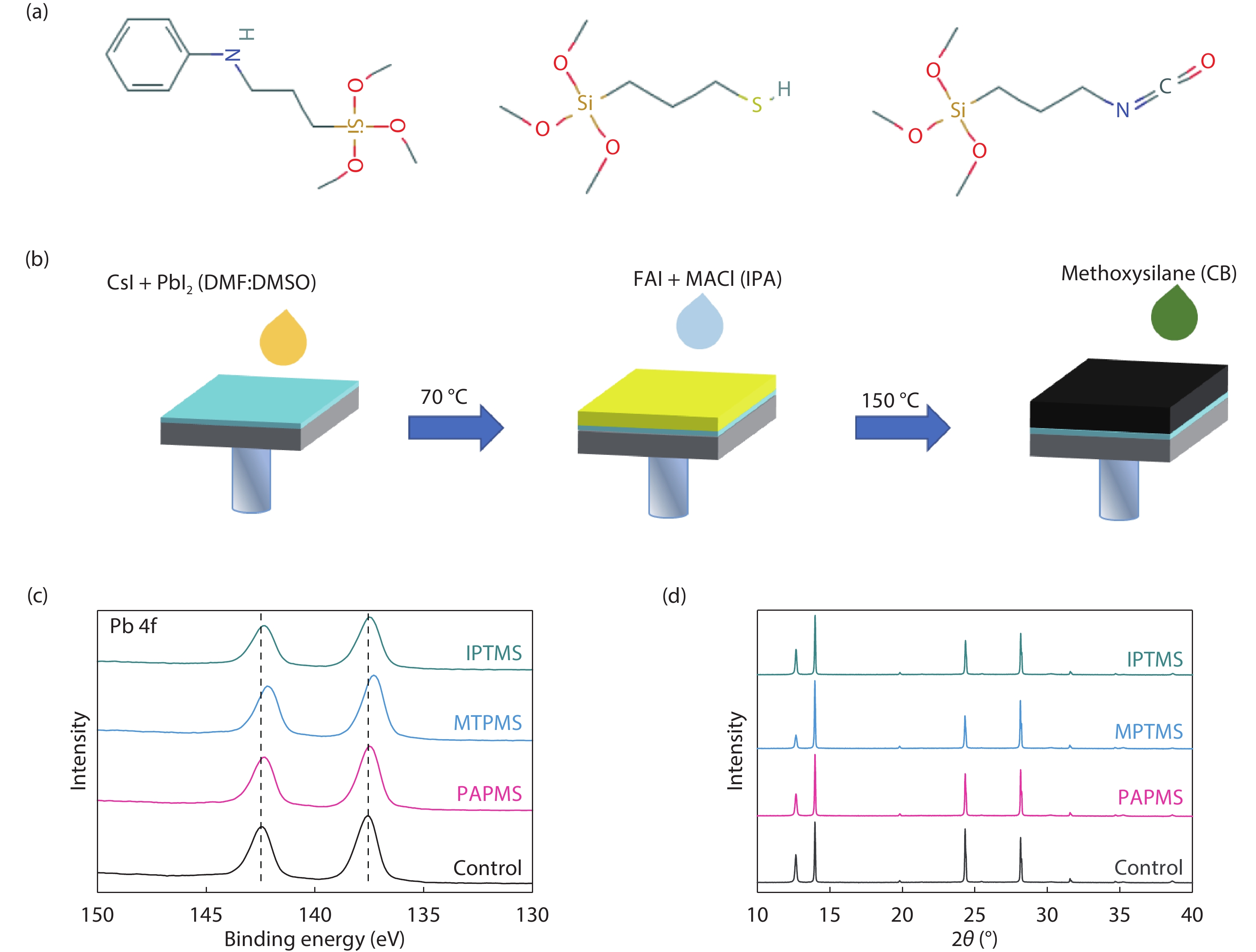
Chemical structures of methoxysilane employed in this work are shown in Fig. 1(a). Previous research has proved that sulfhydryl, carbonyl and aniline groups have a strong interaction with perovskites and can effectively passivate defects. Inspired by these results, we selected three silanes with different terminal functional groups to study the effect of surface functionalization on device performance and long-term stability. The perovskite polycrystalline films are prepared using a two-step spin-coated method and the schematic is depicted in Fig. 1(b). The methoxysilane molecular is dissolved in chlorobenzene solution, and spin-coated on the surface of perovskite films to form the passivation layer.
![]()
Figure 1.(Color online) (a) Chemical structure of PAPMS, MPTMS and IPTMS passivation layer used in this work. (b) Schematic illustration of the formation process of perovskite films based on a sequential deposition. (c) XPS spectra of Pb 4f for the perovskite films with and without siloxane treatment. (d) XRD pattern of perovskite films with and without siloxane treatment.
X-ray photoelectron spectroscopy (XPS) measurement is conducted to verify the interaction between the siloxane and uncoordinated Pb atom. As shown in Fig. 1(c), the peaks at 142.5 and 137.6 eV in the control sample are correspond to Pb2+ 4f7/2 and Pb2+ 4f5/2, respectively, which are not shifted with PAPMS treatment but shifted into a lower binding energy after depositing the IPTMS and MPTMS layer. The shift to a lower binding energy is attributed to electron donation from sulfhydryl and carbonyl groups. We further investigate the crystalline structure of perovskite films with and without siloxane post-treatment by X-ray diffraction (XRD) measurement. As expected, all samples exhibited the similar characteristic diffraction peak positions and intensity, indicating that the crystallinity of perovskite films has not been changed through siloxane surface treatment.
The effects of surface methoxysilane treatment on the photovoltaic performance are estimated with device architecture of ITO/SnO2/FACsPbI3/Spiro-OMeTAD/Au (ITO: indium tin oxide; Spiro-OMeTAD: 2,2′,7,7′-tetrakis (N, N-dipmethoxyphenylamine) - 9,9′-spirobifluorene). We first investigated the dependence of device performance on PAPMS, MPTMS and IPTMS concentration, and the results are plotted in Fig. S1–S3. After optimizing the treatment condition, the device modified with IPTMS exhibited a significantly increased PCE, while PAPMS treatment have a negative impact on device performance (Figs. 2(a)−2(d)). It can be found that the increased performance for IPTMS treated devices is attributed to the improvement of open-circuit voltage (Voc), short-circuit current density (Jsc) and fill factor (FF). Additionally, after introducing MPTMS, the devices exhibit the improved Voc but decreased FF, suggesting that passivated with -SH can minimize surface trap density successfully. These results confirm that the terminal group plays a critical role in the final performance of PSCs.
![]()
Figure 2.(Color online) Photovoltaic performance distribution of PSCs with different termination groups of methoxysilane (a) PCE, (b) open-circuit voltage (
We further prepared control and target devices with anti-refractive coating on the ITO surface, and the J−V curve of champion devices modified with different methoxysilane are plotted in Fig. 2(e). The correspond photovoltaic parameters are listed in Table 1. The best performance of control device exhibits a Voc of 1.088 V, Jsc of 24.84 mA/cm2 and FF of 76.82%, yielding a PCE of 20.78%. In contrast, the device passivated with IPTMS displays a higher efficiency with a Voc of 1.12 V, Jsc of 25.10 mA/cm2 and FF of 78.44%, as a consequence of a promoted PCE up to 21.97%. The integrated current density of control- and IPTMS-treated devices from external quantum efficiency (EQE) spectra are 23.90 and 23.97 mA/cm2, respectively. These results are in good agreement with previous results in J−V curves. We further test the steady-state output power of devices at their maximum power point (Figs. 2(f) and 2(g)). The devices yield stabilized PCE of 20.97% for the control and 21.87% for the IPTMS device.
To elucidate the difference in performance of PSCs treated with different methoxy silane, the photoluminescent (PL) mapping spectra with 450 nm excitation is conducted as shown in Fig. 3(a). The PL intensity of control film presented an inhomogeneous distribution. However, the film with PAPMS treatment showed a wider distribution with lower luminescence intensity than control, corresponding to the damage effects of its on-device performance. In addition, we find that the intensity of films become stronger and more uniform after MPTMS and IPTMS treatment. The enhanced PL intensity indicates that surface non-radiative recombination is suppressed by IPTMS passivation.
![]()
Figure 3.(Color online) (a) PL emission intensity mapping of control, PAPMS, MPTMS and IPTMS treated films. (b) EIS spectra of devices based on the pristine and IPTMS treatment. (c) Normalized TPC decay curves for control- and IPTMS-treated devices. (d) Dark
We further in-depth study the mechanisms for the performance enhancement-induced IPTMS surface treatment. The electrochemical impedance spectroscopy (EIS) is performed to investigate the interfacial charge transfer and transport kinetics. As shown in Fig. 3(b), the semicircle at high frequency is ascribed to the carrier recombination at the interface, while the arc at low frequency represents carrier transport in the bulk[
Then, the transient photocurrent (TPC) measurement was conducted to examine the charge transport property of PSCs (Fig. 3(c)). The charge transport constants (τt) slightly decrease from 218.1 to 115.3 μs after methoxysilane treatment, which is ascribed to the promotion of carrier extraction from the perovskite to hole transport layer. These results in agreement with the increasement of Jsc after siloxane treatment. What is more, the space-charge limited current (SCLC) method was further employed to understand the effect of IPTMS passivation on perovskite defect density. The dark J−V curves of devices with structure of ITO/perovskite/Au are plotted in Fig. 3(c). There are three distinct regions can be identified in the J−V curve: an ohmic region with an order n = 1; a child region with n = 2 and a trap-filled limited (TFL) region with n > 3. The trap-filled limit voltage ( VFTL) is always used to estimate the trap density according to the equation of:
where e is elementary charge, nt is the trap density, L is the thickness of perovskite film, ε0 is the vacuum dielectric constant, and ε is the relative dielectric constant of perovskite (46.9 for FAPbI3). The VTFL of the control and target device are 0.44 and 0.61, respectively. As expected, the trap density is reduced from 3.75 × 1015 cm–3 for the control device to 2.70 × 1015 cm–3 for the target device, which benefits the Voc and FF. As mentioned above, we have shown that IPTMS treatment can effectively promote the carrier transportation and reduce the trap density of PSCs, with the better photovoltaic parameters compared with control devices.
To examine whether the IPTMS treatment can prevent perovskite degradation, the long-term thermal stability test for devices with and without IPTMS passivation is also conducted at 85 °C in nitrogen. Thermally stable mixed transport layer is adopted as the HTM to avoid the impact of transport layer degradation on the device stability tracking. The initial PCE of control, MPTMS-treated and IPTMS-treated are 19.14%, 19.32% and 19.81%, respectively. The evolution of photovoltaic performance parameters for control, MPTMS-treated and IPTMS-treated device aged under thermal condition are plotted in Fig. 4. Surprisingly, the IPTMS-treated device presents excellent thermal stability and the remaining 90.4% of its initial PCE after 1500 h storage, whereas the control device is degraded more than 40% exposed under the same condition. Additionally, the MPTMS-treated device also exhibits better long-term thermal stability than the control device, which maintained near 80% of its initial PCE after 1500 h exposure. These results indicate that different termination groups in crosslink methoxysilane also play an important role in device long-term lifetime.
![]()
Figure 4.(Color online) Long-term thermal stability of unsealed devices based on pristine, MPTMS and IPTMS treatment (a) PCE, (b)
We believe the improved of thermal stability by IPTMS is likely stemmed from the improved interface between perovskite/HTL. According to the evolution of performance parameters of MPTMS- and IPTMS-treated devices aging at 85 °C in nitrogen (Fig. 4), the MPTMS-treated device shows an obvious drop in FF and Voc, but the IPTMS-treated device only presents a slight decline in FF and Voc. Generally, FF and Voc are closely related to the interface characteristics. It indicates that the IPTMS-treated device can maintain better interface contact between the perovskite and hole transport layer than the MPTMS-treated device during a continuous heating process.
What is more, we also tested the humidity stability of devices at 60% RH to examine the protective effect of IPTMS molecule on phase transition. However, the performance of unencapsulated devices degraded rapidly (Fig. S4). The PCE of untreated device decreased from 20.63% to 15.02%, which only retained 73% of its initial performance after 24 h ageing. Although the IPTMS-treated devices have better humidity stability, their PCE has also dropped by nearly 10% at the same storage condition. We guessed that the decreased PCE was ascribed to the destroyed of hole transport materials and the phase transition of FACs-based perovskites. Therefore, we should encapsulate the device or select the more stable HTM materials to further improve the humidity stability.
4. Conclusion
In summary, we introduced an effective passivation layer using a silane coupling agent and systematically investigated the effects of terminal groups on photovoltaic performance. Among the investigated methoxysilane, the IPTMS with carbonyl group exhibited the best performance and long-term thermal stability. The PL mapping results show that the passivation layer can significantly reduce the non-radiative recombination loss. Through the EIS and TPC measurements, we found that the carrier transportation has been improved after IPTMS treatment. As a result, the device with IPTMS presented a PCE of 21.97%, higher than 20.97% for the control device. In addition, the excellent thermal stability also has been observed after siloxane surface passivation, retaining nearly 90% of its initial PCE after 1500 h storage.
Acknowledgements
The authors acknowledge funding support from National Natural Science Foundation of China (21975028, 22011540377), National Science Foundation for Young Scientists No. 21805010, Beijing Municipal Science and Technology Project No. Z181100005118002, and Beijing Municipal Natural Science Foundation (JQ19008).
Appendix A. Supplementary materials
Supplementary materials to this article can be found online at https://doi.org/1674-4926/42/11/112201.
References
[1] J H Im, I H Jang, N Pellet et al. Growth of CH3NH3PbI3 cuboids with controlled size for high-efficiency perovskite solar cells. Nat Nanotechnol, 9, 927(2014).
[2] S Y Sun, T Salim, N Mathews et al. The origin of high efficiency in low-temperature solution-processable bilayer organometal halide hybrid solar cells. Energy Environ Sci, 7, 399(2014).
[3] Q F Dong, Y J Fang, Y C Shao et al. Electron-hole diffusion lengths > 175
[4] D Shi, V Adinolfi, R Comin et al. Low trap-state density and long carrier diffusion in organolead trihalide perovskite single crystals. Science, 347, 519(2015).
[5] S D Stranks, G E Eperon, G Grancini et al. Electron-hole diffusion lengths exceeding 1 micrometer in an organometal trihalide perovskite absorber. Science, 342, 341(2013).
[6] N L Chang, A W Yi Ho-Baillie, P A Basore et al. A manufacturing cost estimation method with uncertainty analysis and its application to perovskite on glass photovoltaic modules. Prog Photovolt: Res Appl, 25, 390(2017).
[7]
[8] A Kojima, K Teshima, Y Shirai et al. Organometal halide perovskites as visible-light sensitizers for photovoltaic cells. J Am Chem Soc, 131, 6050(2009).
[9] H S Kim, C R Lee, J H Im et al. Lead iodide perovskite sensitized all-solid-state submicron thin film mesoscopic solar cell with efficiency exceeding 9%. Sci Rep, 2, 591(2012).
[10] H P Zhou, Q Chen, G Li et al. Interface engineering of highly efficient perovskite solar cells. Science, 345, 542(2014).
[11] Q Jiang, Y Zhao, X W Zhang et al. Surface passivation of perovskite film for efficient solar cells. Nat Photonics, 13, 460(2019).
[12] M Jeong, I W Choi, E M Go et al. Stable perovskite solar cells with efficiency exceeding 24.8% and 0.3-V voltage loss. Science, 369, 1615(2020).
[13] W J Yin, T T Shi, Y F Yan. Unusual defect physics in CH3NH3PbI3 perovskite solar cell absorber. Appl Phys Lett, 104, 063903(2014).
[14] T S Sherkar, C Momblona, L Gil-Escrig et al. Recombination in perovskite solar cells: Significance of grain boundaries, interface traps, and defect ions. ACS Energy Lett, 2, 1214(2017).
[15] M Yavari, M Mazloum-Ardakani, S Gholipour et al. Reducing surface recombination by a poly(4-vinylpyridine) interlayer in perovskite solar cells with high open-circuit voltage and efficiency. ACS Omega, 3, 5038(2018).
[16] J P Correa-Baena, W Tress, K Domanski et al. Identifying and suppressing interfacial recombination to achieve high open-circuit voltage in perovskite solar cells. Energy Environ Sci, 10, 1207(2017).
[17] D Y Son, J W Lee, Y J Choi et al. Self-formed grain boundary healing layer for highly efficient CH3NH3PbI3 perovskite solar cells. Nat Energy, 1, 16081(2016).
[18] G Tumen-Ulzii, C J Qin, D Klotz et al. Detrimental effect of unreacted PbI2 on the long-term stability of perovskite solar cells. Adv Mater, 32, 1905035(2020).
[19] T H Liu, Y Y Zhou, Z Li et al. Stable formamidinium-based perovskite solar cells via
[20] R J Sutton, G E Eperon, L Miranda et al. Bandgap-tunable cesium lead halide perovskites with high thermal stability for efficient solar cells. Adv Energy Mater, 6, 1502458(2016).
[21] J W Lee, D H Kim, H S Kim et al. Formamidinium and cesium hybridization for photo- and moisture-stable perovskite solar cell. Adv Energy Mater, 5, 1501310(2015).
[22] Y Zhang, S Seo, S Y Lim et al. Achieving reproducible and high-efficiency (> 21%) perovskite solar cells with a presynthesized FAPbI3 powder. ACS Energy Lett, 5, 360(2020).
[23] H Wang, C Zhu, L Liu et al. Interfacial residual stress relaxation in perovskite solar cells with improved stability. Adv Mater, 31, 1904408(2019).
[24] S Yang, S S Chen, E Mosconi et al. Stabilizing halide perovskite surfaces for solar cell operation with wide-bandgap lead oxysalts. Science, 365, 473(2019).
[25] Z H Zhang, J Li, Z M Fang et al. Adjusting energy level alignment between HTL and CsPbI2Br to improve solar cell efficiency. J Semicond, 42, 030501(2021).
[26] Z M Fang, X Y Meng, C T Zuo et al. Interface engineering gifts CsPbI2.25Br0.75 solar cells high performance. Sci Bull, 64, 1743(2019).
[27] F Wan, L L Ke, Y B Yuan et al. Passivation with crosslinkable diamine yields 0.1 V non-radiative
[28] M Cheng, C T Zuo, Y Z Wu et al. Charge-transport layer engineering in perovskite solar cells. Sci Bull, 65, 1237(2020).
[29] L F Zhu, Y Z Xu, P P Zhang et al. Investigation on the role of Lewis bases in the ripening process of perovskite films for highly efficient perovskite solar cells. J Mater Chem A, 5, 20874(2017).
[30] Y C Shao, Z G Xiao, C Bi et al. Origin and elimination of photocurrent hysteresis by fullerene passivation in CH3NH3PbI3 planar heterojunction solar cells. Nat Commun, 5, 5784(2014).
[31] J X Xu, A Buin, A H Ip et al. Perovskite–fullerene hybrid materials suppress hysteresis in planar diodes. Nat Commun, 6, 7081(2015).
[32] X P Zheng, B Chen, J Dai et al. Defect passivation in hybrid perovskite solar cells using quaternary ammonium halide anions and cations. Nat Energy, 2, 1(2017).
[33] H R Tan, A Jain, O Voznyy et al. Efficient and stable solution-processed planar perovskite solar cells via contact passivation. Science, 355, 722(2017).
[34] A Rajagopal, R J Stoddard, S B Jo et al. Overcoming the photovoltage plateau in large bandgap perovskite photovoltaics. Nano Lett, 18, 3985(2018).
[35] D Yang, X Zhou, R X Yang et al. Surface optimization to eliminate hysteresis for record efficiency planar perovskite solar cells. Energy Environ Sci, 9, 3071(2016).


Set citation alerts for the article
Please enter your email address

© Copyright 2018-2021 | Chinese Laser Press. All Rights Reserved 沪ICP备15018463号-20